
Fuse and method for disconnecting the fuse

Inactive Publication Date: 2007-04-26
FUJITSU SEMICON LTD
View PDF14 Cites 34 Cited by
  • Summary
  • Abstract
  • Description
  • Claims
  • Application Information

AI Technical Summary

Benefits of technology

[0009] An object of the present invention is to provide a fuse which can prevent inter-layer insulating film from cracking without making the fuse circuit large and can have a large resistance change between before and after the disconnection of the fuse, and a method for disconnecting the fuse.
[0014] According to further another aspect of the present invention, there is provided a method for disconnecting a fuse comprising an interconnection part including a silicon layer; a first contact part connected to one end of the interconnection part; and a second contact connected to the other end of the interconnection part and containing a metal material, a current being flowed from the first contact part to the second contact part via the interconnection part to migrate the metal material of the second contact part to the silicon layer to thereby change a connection resistance between the interconnection part and the second contact part.
[0015] According to further another aspect of the present invention, there is provided a method for disconnecting a fuse comprising an interconnection part including a silicon layer and a metal silicide layer formed on the silicon layer; a first contact part connected to one end of the interconnection part; and a second contact part connected to the other end of the interconnection part, a current being flowed from the first contact part to the second contact part via the interconnection part to migrate a metal material forming the metal silicide layer to a side of the first contact part to thereby change a contact resistance between the interconnection part and the second contact part.
[0016] According to the present invention, the fuse comprises an interconnection part including a silicon layer, a first contact part connected to one end of the interconnection part; and a second contact part connected to the other end of the interconnection part and containing a metal material, and a current is flowed from the first contact part to the second contact part to migrate the metal material of the second contact part to the silicon layer to thereby disconnect the fuse, whereby the peripheral elements can be kept from being damaged upon the disconnecting. Thus, the cracking of the inter-layer insulating film can be prevented without making the fuse circuit large. The first contact part and the second contact part can be completely disconnected from each other by migrating the metal material of the second contact part, whereby the resistance change between before and after the disconnecting can be large.

Problems solved by technology

In such case, if the defective partial circuit or memory cell makes the whole device defective, it will lower the fabrication yield, which will lead to the fabrication cost increase.
However, the method of flowing current to melt off the fuse, which requires high current for melting off the polycrystalline silicon and making the transistors for controlling the current and the interconnection for supplying the current large, makes it difficult to downsize the fuse circuit.
Explosions occurring in melting off the fuse often crack the inter-layer insulating film on the fuse.
The cracks, if grow, are extended to the interconnection layers near the fuse in the worst case, resultantly causing problems of the disconnection of the interconnection layers, etc.
To prevent the inter-layer insulating film from cracking, it is effective provide a guard ring, which disadvantageously increases the area of the fuse circuit.
Accordingly, the resistance increase of the fuse portion is about 10 times at most, and it is difficult to judge the disconnection of the fuse.

Method used


Image

  • Fuse and method for disconnecting the fuse
  • Fuse and method for disconnecting the fuse
  • Fuse and method for disconnecting the fuse

Examples


first embodiment

[0032] [A First Embodiment]

[0033] The fuse and the method for disconnecting the fuse according to a fist embodiment of the present invention will be explained with reference to FIGS. 1 to 6B.

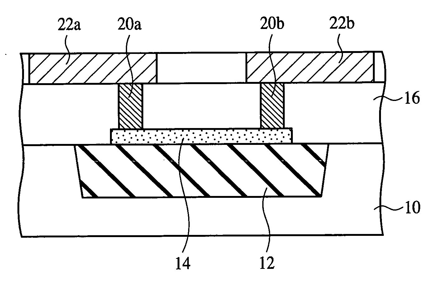
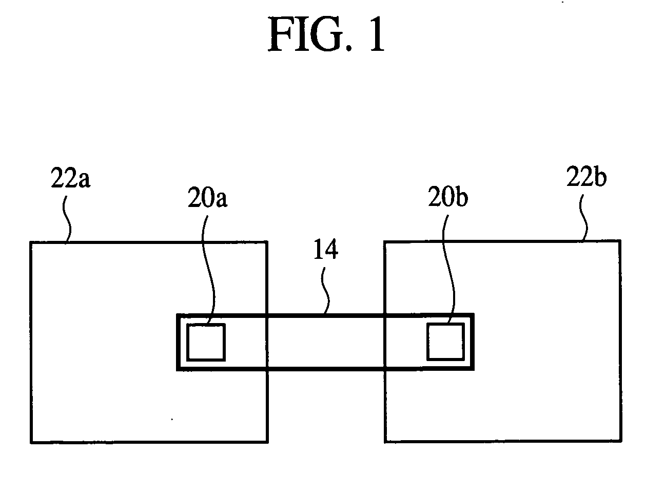
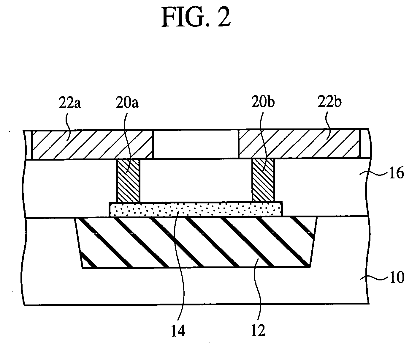
[0034]FIG. 1 is a plan view of the fuse according to the present embodiment. FIG. 2 is a diagrammatic sectional view of the fuse according to the present embodiment. FIG. 3 is a circuit diagram of one example of the fuse circuit. FIG. 4 is a diagrammatic sectional view showing the method for disconnecting the fuse according to the present embodiment. FIGS. 5A-5C and 6A-6B are sectional views of the fuse according to the present embodiment in the steps of the method for fabricating the same.

[0035] First, the structure of the fuse according to the present embodiment will be explained with reference to FIGS. 1 and 2.

[0036] A device isolation film 12 defining active regions is formed in the primary surface of a silicon substrate 10. An interconnection part 14 of polycrystalline silicon is formed ...


PUM


Abstract

The fuse comprises an interconnection part 14 luding a silicon layer; a contact part 20b connected one end of the interconnection part 14; and a contact part 20aconnected to the other end of the interconnection part 14 and containing a metal material. A current is flowed from the contact part 20bto the contact part 20a to migrate the metal material of the contact part 20a to the silicon layer to thereby change the contact resistance between the interconnection part 14 and the contact part 20a.

Description

CROSS-REFERENCE TO RELATED APPLICATIONS [0001] This application is based upon and claims the benefit of priority from the prior Japanese Patent Application No. 2005-255977, filed on Sep. 5, 2005, the entire contents of which are incorporated herein by reference. BACKGROUND OF THE INVENTION [0002] The present invention relates to a fuse and a method for disconnecting the fuse, more specifically a fuse which can electrically disconnect and reconstruct a circuit, and a method for disconnecting the fuse. [0003] A semiconductor device, such as a memory device, e.g., DRAM, SRAM or others, or a logic device or others, comprises a very large number of devices, and often a partial circuit or memory cell does not normally operate due to various factors of the fabrication process. In such case, if the defective partial circuit or memory cell makes the whole device defective, it will lower the fabrication yield, which will lead to the fabrication cost increase. To prevent this, recently in semi...

Claims


Application Information

Patent Timeline
IPC IPC(8): H01L29/00
CPCH01L23/5256H01L2924/0002H01L2924/00Y02B20/40
Inventor OTSUKA, SATOSHISAWADA, TOYOJISUGA, MASATONAGAYAMA, JUNSATO, MOTONOBUSUZUKI, TAKASHI
Owner FUJITSU SEMICON LTD
Learn More