Wafer-to-wafer stack with supporting pedestal

a stack and supporting pedestal technology, applied in the direction of electrical apparatus, semiconductor devices, semiconductor/solid-state device details, etc., can solve the problems of increasing the design increasing the size of chips, and increasing the complexity of integrated circuits. , to achieve the effect of high thermal conductivity

Active Publication Date: 2007-04-26
IND TECH RES INST
View PDF4 Cites 45 Cited by
  • Summary
  • Abstract
  • Description
  • Claims
  • Application Information

AI Technical Summary

Benefits of technology

[0038] Based on the above, a novel three dimensional wafer stack structure and the manufacturing method therefor are provided. In Comparison with the conventional three dimensional wafer stack, the three dimensional wafer stack structure according to the present invention is further provided with at least one pedestal arranged in each chip area of the device layer for preventing the low-k materials existing in the device layer from being damaged by the stresses. Moreover, the pedestals, which are usually formed by a metal material having a relatively high thermal conductivity, constructed by a columnar structure or a lateral structure, and can run through the first and the second substrates, are also used as the thermal conductive devices, in order to release the heat generated in the device layers.

Problems solved by technology

Under such a development trend, the size of the chip used for the electronic products should be miniaturized, but the integrated circuits contained in the chip are becoming more and more complicated.
However, advancing scaling down of chip size and increasing the design complexity of the integrated circuits entail a multiplicity of problems, such as, the crosstalk effect and the thermal issues on the chip, or the proximity effect in the lithography and etching processes.
However, a new problem may occur in such a three dimensional wafer stack structure.
The low-k materials, which exist in the respective device layer and are used for allowing the conducting wires thereof being arranged closely, might be destroyed by compression stresses resulting from the stacking structure or by the thermal stresses resulting from the heat generated by the circuit devices.

Method used


Image

  • Wafer-to-wafer stack with supporting pedestal
  • Wafer-to-wafer stack with supporting pedestal
  • Wafer-to-wafer stack with supporting pedestal

Examples


Embodiment Construction

[0047] The present invention will now be described more specifically with reference to the following embodiments. It is to be noted that the following descriptions of preferred embodiments of this invention are presented herein for purpose of illustration and description only; it is not intended to be exhaustive or to be limited to the precise form disclosed.

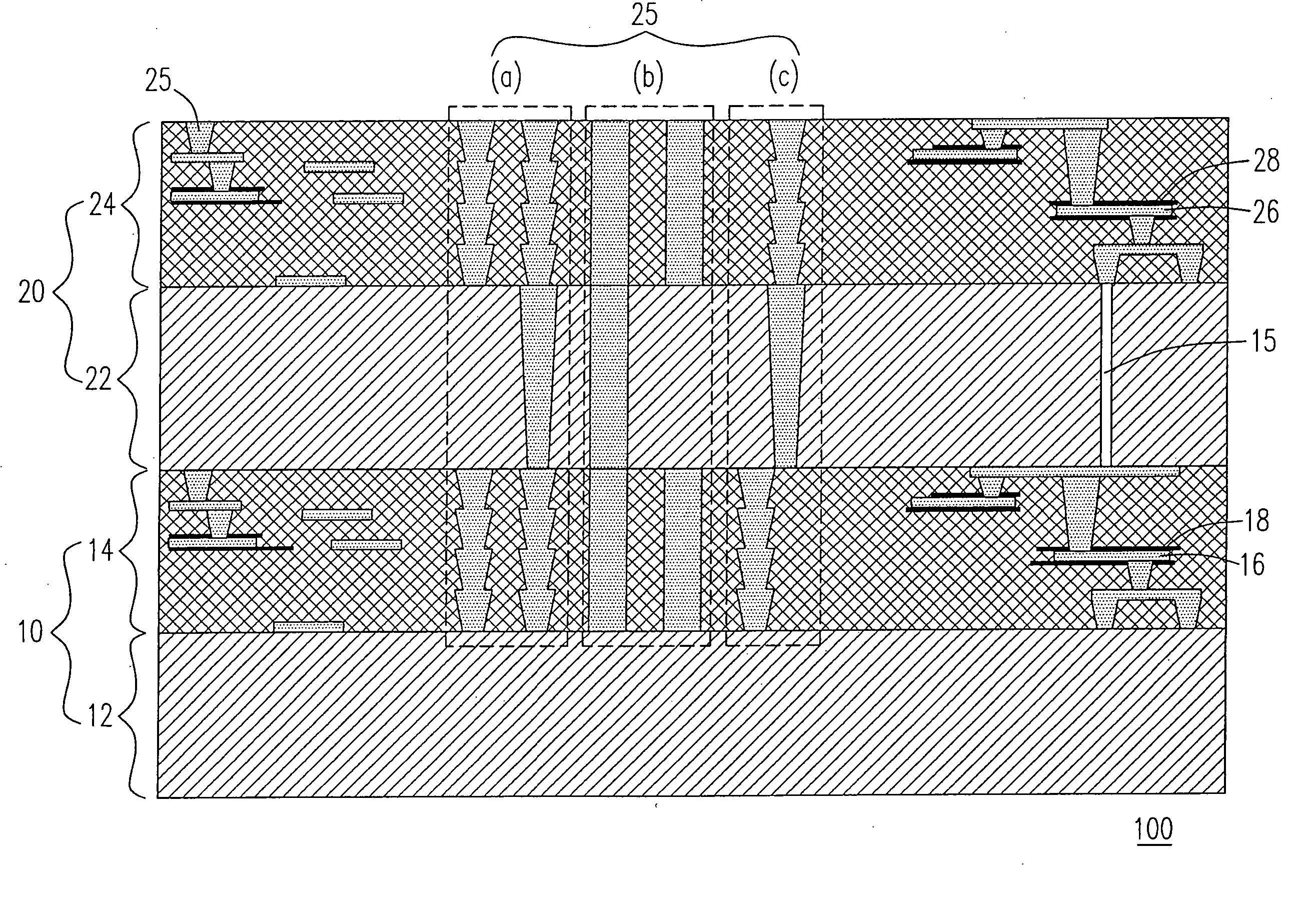
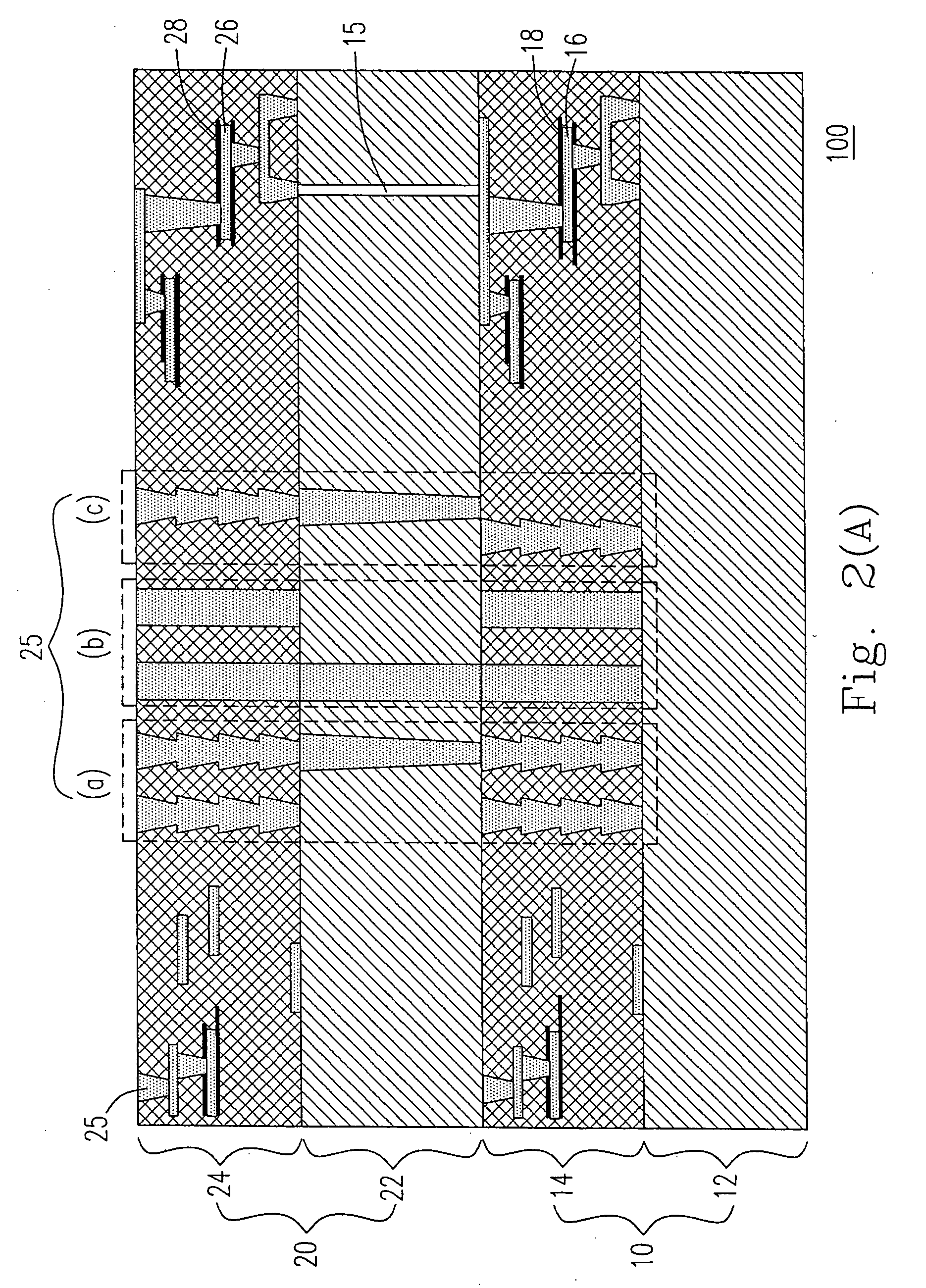
[0048] Please refer to FIGS. 2(A)-2(D), which respectively shows the different embodiments of the three dimensional wafer stack according to the present invention. As can be seen from FIG. 2(A), the three dimensional wafer stack 100 according to a first embodiment of the present invention includes a first wafer 10 and a second wafer 20, both of which are arranged face-up, so as to configure the first and the second wafers 10, 20 as a back to face (or back to front) wafer stack. Specifically, the first and the second wafers 10, 20 further include a first and a second substrates 12, 22 as well as a first and a second device layer...


PUM


Abstract

A novel three dimensional wafer stack and the manufacturing method therefor are provided. The three dimensional wafer stack includes a first wafer having a first substrate and a first device layer having thereon at least one chip, a second wafer disposed above the first wafer and having a second substrate, and at least one pedestal arranged between and extending from the first substrate to the second substrate. The pedestal arranged in the device layer is used for preventing the low-k materials existing in the device layer from being damaged by the stresses.

Description

FIELD OF THE INVENTION [0001] The present invention relates to a wafer stack structure, and in particular to a three dimensional wafer stack having at least one supporting pedestal formed therein. BACKGROUND OF THE INVENTION [0002] As the rapid development of the semiconductor process, more and more electronic products can be provided with higher performance, higher portability and more compactness. Under such a development trend, the size of the chip used for the electronic products should be miniaturized, but the integrated circuits contained in the chip are becoming more and more complicated. However, advancing scaling down of chip size and increasing the design complexity of the integrated circuits entail a multiplicity of problems, such as, the crosstalk effect and the thermal issues on the chip, or the proximity effect in the lithography and etching processes. Recently, a novel three dimensional wafer structure design has been gradually developed in order to overcome the probl...

Claims


Application Information

Patent Timeline
Patent Type & Authority Applications(United States)
IPC IPC(8): H01L23/12H01L21/58
CPCH01L23/481H01L23/552H01L23/562H01L23/60H01L23/642H01L24/94H01L25/0657H01L2225/06513H01L2225/06541H01L2225/06572H01L2924/01005H01L2924/01006H01L2924/01019H01L2924/01033H01L23/49827H01L2924/12042H01L2924/14H01L2924/351H01L2924/00
Inventor CHANG, CHI-SHIHTAIN, RA-MINLIAU, SHYI-CHINGLO, WEI-CHUNGLEE, RONG-SHEN
Owner IND TECH RES INST
Why Eureka
Try Eureka