Exclusion zone for stress-sensitive circuit design

a technology of stress-sensitive circuits and exclusion zones, which is applied in the field of integrated circuits, can solve the problems of affecting the reliability of the integrated circuit, the performance of the device is affected, and the method has a side effect, so as to improve the the performance and reliability of the integrated circuit containing the stress-sensitive circuit is improved, and the process steps or costs are not extra.

Active Publication Date: 2007-04-26
TAIWAN SEMICON MFG CO LTD
View PDF98 Cites 14 Cited by
  • Summary
  • Abstract
  • Description
  • Claims
  • Application Information

AI Technical Summary

Benefits of technology

[0008] In accordance with one aspect of the present invention, the semiconductor structure includes a semiconductor chip. Stress-sensitive circuits are substantially excluded out of an exclusion zone on the chip to reduce the effects of the stress to the stress-sensitive circuits. The stress-sensitive circuits are preferably analog circuits. The exclusion zone preferably includes corner regions of the semiconductor chip, wherein the corner regions preferably have a diagonal length of less than about one percent of the diagonal length of the semiconductor chip.
[0012] The advantageous features of the preferred embodiments of the present invention include full compatibility with existing integrated circuit fabrication processes with no extra process steps or cost involved. The performance and reliability of integrated circuits containing stress-sensitive circuits are improved.

Problems solved by technology

These methods have a side effect, however.
Not only is the performance of the devices affected, but undesired stress may also cause a malfunction of the semiconductor devices, affecting the reliability of the integrated circuit.
Thinner dies, on the other hand, have increased stresses, further worsening the problem.
However, due to the demand for thin dies, these methods have become less practical.
Additionally, modification to packaging processes requires testing and debugging, thus increasing the cost and time to market.

Method used


Image

  • Exclusion zone for stress-sensitive circuit design
  • Exclusion zone for stress-sensitive circuit design
  • Exclusion zone for stress-sensitive circuit design

Examples


Embodiment Construction

[0020] The making and using of the presently preferred embodiments are discussed in detail below. It should be appreciated, however, that the present invention provides many applicable inventive concepts that can be embodied in a wide variety of specific contexts. The specific embodiments discussed are merely illustrative of specific ways to make and use the invention, and do not limit the scope of the invention.

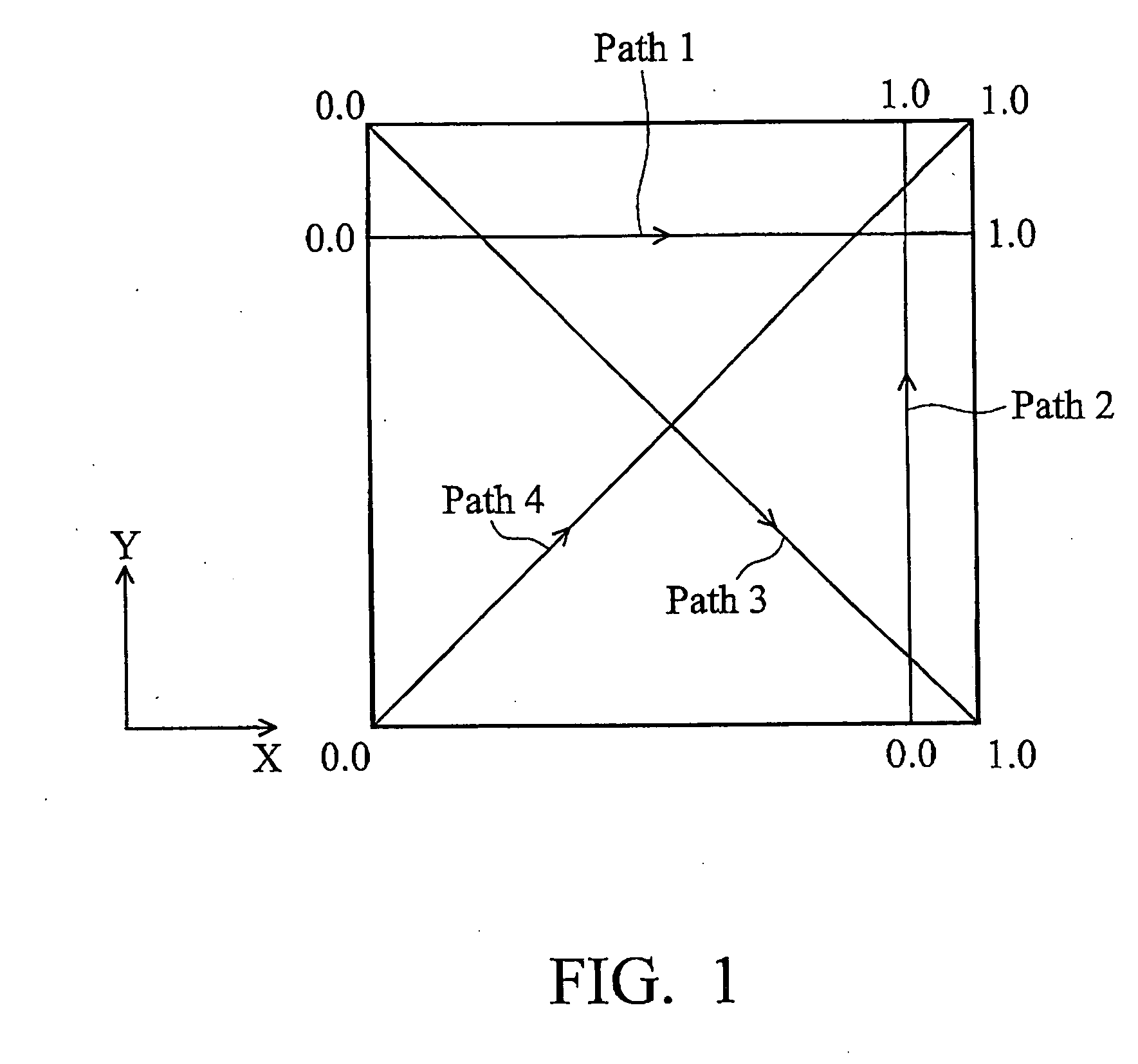
[0021] Research has been conducted to analyze the stress on chips. FIG. 1 illustrates a semiconductor chip. Four paths, path 1, path 2, path 3 and path 4, are provided and respective stresses along the paths on the chip are simulated. Paths 1 and 2 are referred to as straight paths, wherein path 1 is parallel to the X-axis, and path 2 is parallel to the Y-axis. Path 3 and path 4 are diagonal paths along diagonal directions of the chip.

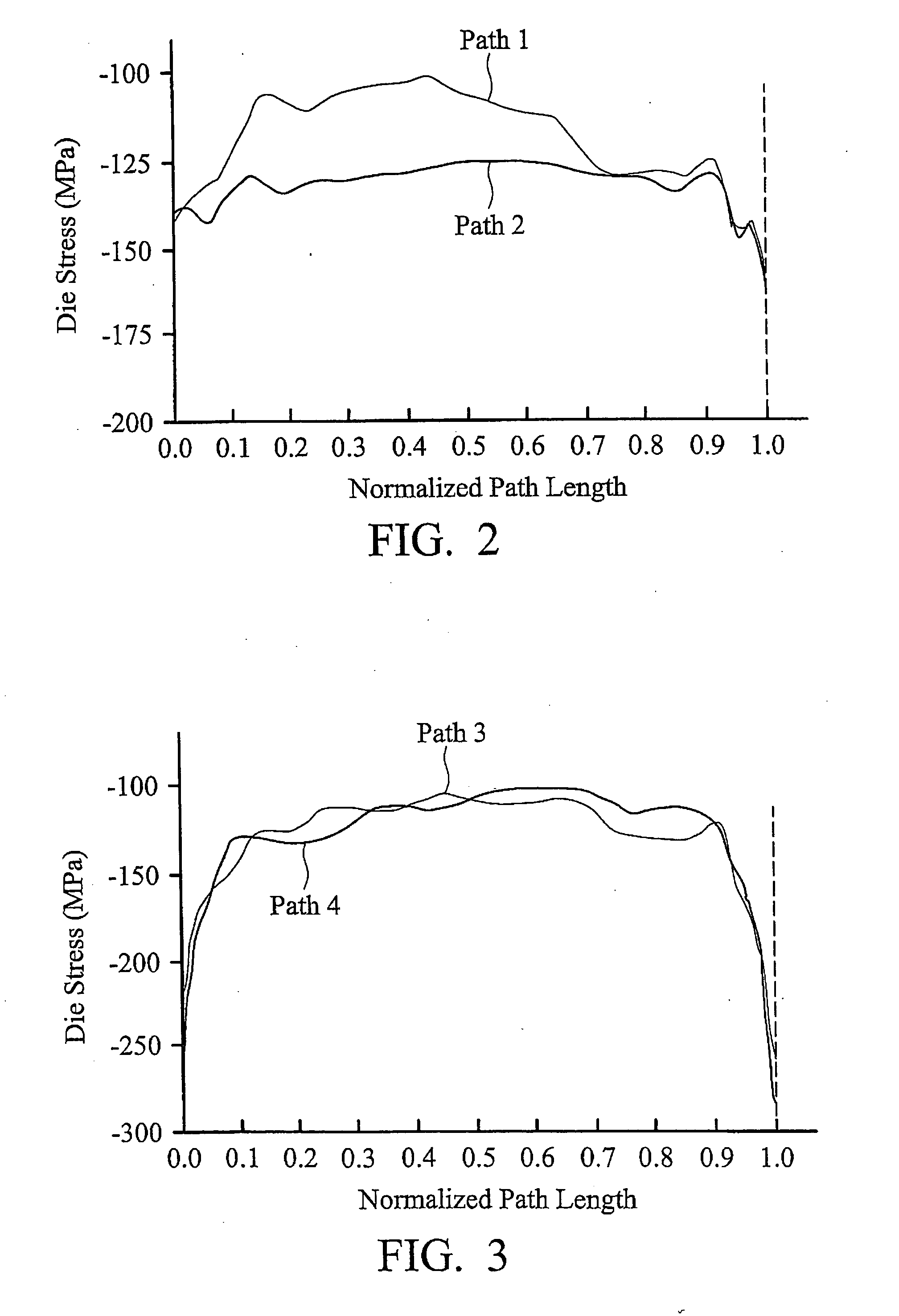
[0022]FIG. 2 illustrates a stress distribution on a sample chip, wherein the die stresses are shown as functions of normalized path lengths ...


PUM


Abstract

A semiconductor structure less affected by stress and a method for forming the same are provided. The semiconductor structure includes a semiconductor chip. Stress-sensitive circuits are substantially excluded out of an exclusion zone to reduce the effects of the stress to the stress-sensitive circuits. The stress-sensitive circuits include analog circuits. The exclusion zone preferably includes corner regions of the semiconductor chip, wherein the corner regions preferably have a diagonal length of less than about one percent of the diagonal length of the semiconductor chip. The stress-sensitive analog circuits preferably include devices having channel lengths less than about five times the minimum channel length.

Description

[0001] This application claims priority to provisional patent application Ser. No. 60 / 725,493; filed on Oct. 11, 2005, entitled “Exclusion Zone for N90 Stress-Sensitive Circuit Design,” which application is incorporated herein by reference.TECHNICAL FIELD [0002] This invention relates generally to integrated circuits, and more particularly to the fabrication of stress-sensitive integrated circuits. BACKGROUND [0003] With the advancement of modem technologies, integrated circuits having more functions and greater performance are increasingly demanded, which requires more semiconductor devices to be made for a circuit. A high degree of integration can be achieved in several ways, among which scaling semiconductor devices is the most commonly used method. Ninety (90)nm, 60 nm, and even 45 nm technologies have been used to produce very small devices having high performance. During packaging processes, two or more dies may be stacked together, and the dies may include integrated circuits...

Claims


Application Information

Patent Timeline
Patent Type & Authority Applications(United States)
IPC IPC(8): H01L23/29
CPCH01L23/522H01L25/50H01L27/0203H01L2225/0651H01L2225/06517H01L2225/06555H01L2225/06582H01L2224/16225H01L2224/48227H01L2924/01327H01L25/0657H01L22/12H01L27/0207H01L2924/00
Inventor SU, CHAO-YUANLIN, CHUNG-YI
Owner TAIWAN SEMICON MFG CO LTD
Why Eureka
Try Eureka