Active matrix display and forming method thereof

a technology of active matrix and forming method, which is applied in the direction of instruments, non-linear optics, optics, etc., can solve the problems of insufficient temperature resistance of the drive circuit and easy contamination, and achieve the effects of reducing stress, minimizing damage to the drive circuit, and high packaging density

Inactive Publication Date: 2009-05-26
SEMICON ENERGY LAB CO LTD
View PDF126 Cites 10 Cited by
  • Summary
  • Abstract
  • Description
  • Claims
  • Application Information

AI Technical Summary

Benefits of technology

[0015]The peripheral driver circuit region is located either within the region where the liquid crystal material exists or within the sealing material. It substantially follows that the peripheral driver circuit region is sealed in the liquid crystal material or in the sealing material. This can prevent extraneous moisture from encroaching on the peripheral driver circuit region of high packaging density. Furthermore, the effects of stress can be mitigated.
[0016]To minimize the damage of a drive circuit in an active matrix liquid crystal display device in a panel assembly process, and to solve the problem of reliability, an active matrix liquid crystal display device is required to be manufactured such that the drive circuit thereof cannot be touched directly. Therefore, a peripheral drive circuit region 803 of an active matrix liquid crystal display device is mounted in liquid crystal or sealing material as shown in FIG. 8.
[0019]Further, in the constitution shown in FIG. 8, the active matrix liquid display device is divided by sealing material 802 so as to realize a manufacturing of a plurality of active matrix liquid crystal display panels on a pair of glass substrates. With such a constitution, the productivity and the reliability can be simultaneously enhanced.

Problems solved by technology

Therefore, the driver circuit does not have sufficient temperature resistance, and is vulnerable to contamination.

Method used


Image

  • Active matrix display and forming method thereof
  • Active matrix display and forming method thereof
  • Active matrix display and forming method thereof

Examples


example 1

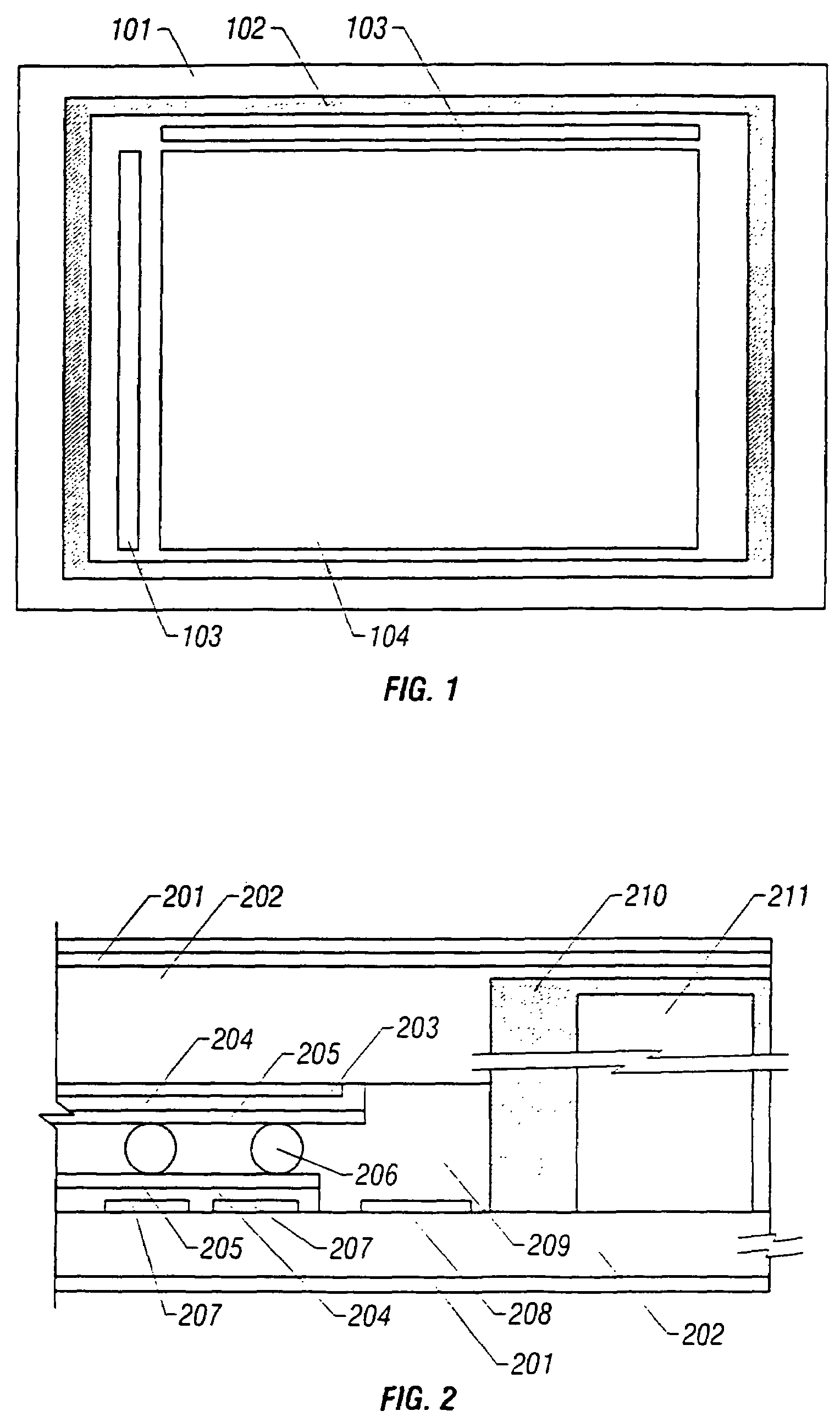
[0039]An active matrix display according to the present invention is shown in FIG. 2 in cross section. This active matrix display has a glass substrate 202 on which pixel TFTs 207 are formed. A transparent electrode 204 and an orientation film 205 are laminated on the pixel TFTs 207. This glass substrate is referred to as the TFT substrate. This TFT substrate comprises a polarizing sheet 201 and the glass substrate 202 which are arrayed in this order in the direction towards a liquid crystal material 209.

[0040]The other glass substrate is referred to as the color filter substrate and comprises an orientation film 205, a transparent electrode 204, color filters 203, a glass substrate 202, and a polarizing sheet 201 which are arrayed in this order in the direction away from the liquid crystal material 209.

[0041]A number of spacers 206 of glass or a resin are dispersed in the liquid crystal material 209 to maintain the spacing between the two glass substrates 202 constant.

[0042]The pol...

example 2

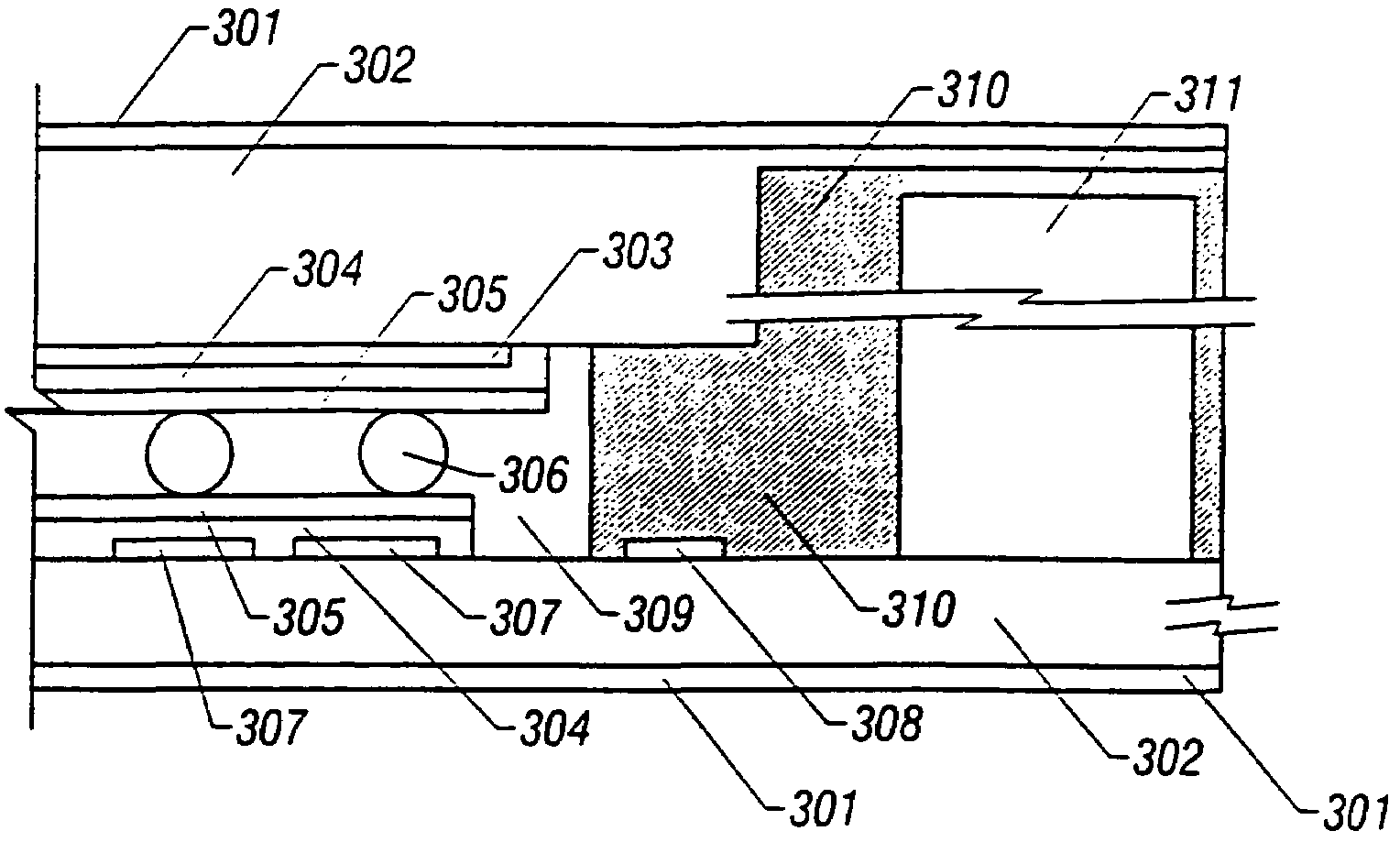
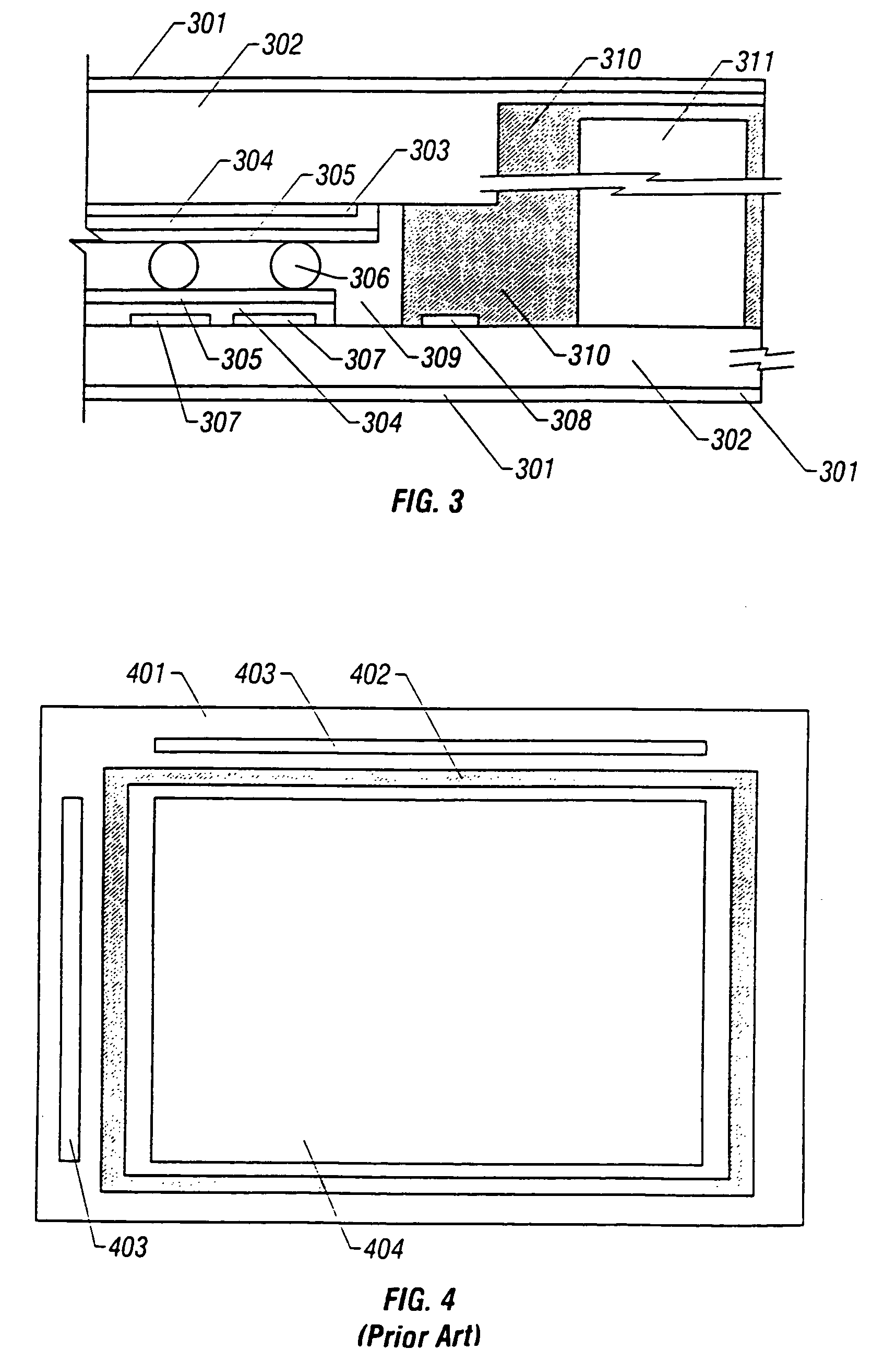
[0069]Another active matrix display according to the present invention is shown in FIG. 3 in cross section. As can be seen from this figure, a microprocessor 311 for controlling the active matrix display and TFTs 308 forming a driver circuit are sealed by a sealing material 310, thus protecting the driver circuit TFTs 308. The driver circuit TFTs 308 are prevented from being exposed. The present example is similar to Example 1 in structure and process sequence except for circuit elements (driver circuit TFTs 308) sealed by the sealing material 310.

example 3

[0070]The present example pertains to a structure equipped with a preliminary peripheral circuit (redundant circuit).

[0071]FIG. 7 is a schematic top view of a liquid crystal panel according to the present example. Since FIG. 7 is a view taken from the top, only one glass substrate 701 is shown. In practice, however, another glass substrate which makes a ˜pair with the glass substrate 701 is bonded to the glass substrate 701. In the structure shown in FIG. 7, a peripheral driver circuit region 703 and a matrix pixel region 704 are located inside a sealing material 702. Since the inside of the sealing material 702 is filled with a liquid crystal material, the liquid crystal material exists on the top surfaces of the TFTs arranged in the peripheral driver circuit region 703 and in the pixel region 704.

[0072]An integrated circuit (IC) forming various control circuits connected with the peripheral driver circuit is positioned within the sealing material 702 and just molded in this sealin...


PUM

PropertyMeasurementUnit
thicknessaaaaaaaaaa
thicknessaaaaaaaaaa
temperatureaaaaaaaaaa

Abstract

An active matrix liquid crystal display having improved reliability. Pixel regions and a peripheral driver circuit are integrally packed on the display. TFTs forming the peripheral driver circuit are located inside a sealing material layer on the side of a liquid crystal material, thus protecting the peripheral driver circuit from external moisture and contaminants. This enhances the long-term reliability of the peripheral driver circuit. Pixel TFTs are arranged in pixel regions. The leads going from the TFTs forming the peripheral driver circuit to the pixel TFTs are shortened. This results in a reduction in the resistance. As a result, the display characteristics are improved.

Description

CROSS-REFERENCE TO RELATED APPLICATION[0001]This application is a divisional application of U.S. application Ser. No. 10 / 037,103, filed on Dec. 31, 2001, now U.S. Pat. No. 6,703,643 which is a divisional of U.S. application Ser. No. 09 / 287,551, filed on Apr. 5, 1999, now U.S. Pat. No. 6,355,942 B1, which is a continuation of U.S. application Ser. No. 08 / 601,956, filed on Feb. 15, 1996, now U.S. Pat. No. 6,011,607, which claims the benefit of foreign priority applications filed in Japan on Feb. 15, 1995 as serial no. 07-50527, and on Mar. 20, 1995 as serial no. 07-87369, and on Dec. 20, 1995 as serial no. 07-349669. This application claims priority to each of these prior applications, and the disclosures of the prior applications are considered part of (and are incorporated by reference in) the disclosure of this application.BACKGROUND OF THE INVENTION[0002]1. Field of the Invention[0003]The present invention relates to techniques for miniaturizing active matrix displays and for enha...

Claims


Application Information

Patent Timeline
Patent Type & Authority Patents(United States)
IPC IPC(8): G02F1/1339G02F1/1362
CPCG02F1/13454G02F1/1339
Inventor YAMAZAKI, SHUNPEIKOYAMA, JUNKAWASAKI, YUJIKONUMA, TOSHIMITSUTERAMOTO, SATOSHIHIRAKATA, YOSHIHARU
Owner SEMICON ENERGY LAB CO LTD
Why Eureka
Try Eureka