GOA circuit, liquid crystal panel and display device

A circuit and circuit point technology, applied in the field of liquid crystal display, can solve the problems of GOA circuit failure, threshold voltage Vth deflection, forward deflection, etc., to reduce the overall pressure effect and improve reliability and stability.

Active Publication Date: 2018-01-19
SHENZHEN CHINA STAR OPTOELECTRONICS SEMICON DISPLAY TECH CO LTD
View PDF10 Cites 10 Cited by
  • Summary
  • Abstract
  • Description
  • Claims
  • Application Information

AI Technical Summary

Problems solved by technology

exist figure 2 Generally, two pull-down sustaining circuits are set up ⑤ to work alternately to prevent the thin-film transistors T32, T42, T33, and T43 from being subject to PBS (Positive Bias Stress) for a long time, which will cause the threshold voltage Vth of the device to deflect seriously cause the circuit to fail
[0006] However, figure 2 The two pull-down sustaining circuits ⑤ use the anti-phase signals LC1 and LC2 respectively, that is, the potentials of LC1 and LC2 are different at the same time, but when LC1 is at a high potential, the pull-down sustaining circuit ⑤ on the left side of the single-stage GOA structural unit works, The gate connection point P(N) of the thin film transistors T42 and T32 is in a high potential state for a long time, thus causing the threshold voltage Vth of the thin film transistors T42 and T32 to be deflected forward; similarly, after a period of time, the potentials of LC1 and LC2 are exchanged , the pull-down maintenance circuit ⑤ on the right side of the single-stage GOA structure unit works, making the gate connection point K (N) of the thin film transistor T43 and T33 stay in a high potential state for a long time, thus causing the threshold voltage Vth of the thin film transistor T43 and T33 to appear positive deflection
Repeating this, as the usage time of the single-stage GOA structural unit increases, the threshold voltage Vth of the thin film transistors T32, T42, T33, and T43 will deflect more and more seriously, resulting in the failure of the entire GOA circuit

Method used


Image

  • GOA circuit, liquid crystal panel and display device
  • GOA circuit, liquid crystal panel and display device
  • GOA circuit, liquid crystal panel and display device

Examples


Embodiment Construction

[0045] In order to make the object, technical solution and advantages of the present invention clearer, the present invention will be further described in detail below in conjunction with the accompanying drawings.

[0046] In Embodiment 1 of the present invention, a GOA circuit is provided, which includes a plurality of cascaded GOA structural units, and each single-level GOA structural unit sends a corresponding row of pixels in the display area of ​​the display panel according to the Nth-level GOA structural unit. The unit outputs row scanning signals. For the convenience of description, the Nth-level GOA structure unit is used for detailed description.

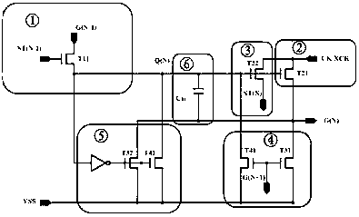
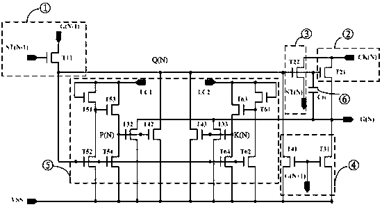
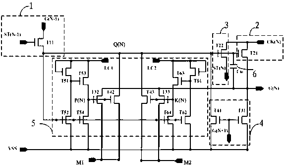
[0047] Such as image 3 As shown, the Nth-level GOA structural unit includes a pull-up control circuit 1, a pull-up circuit 2, a downlink circuit 3, a pull-down circuit 4, a pull-down maintenance circuit 5, and a bootstrap capacitor 6, and N is a positive integer; where,

[0048] The pull-down maintenance circuit 5 includ...


PUM


Abstract

The invention provides a GOA circuit. The GOA circuit comprises multiple GOA structural units which are in cascade connection, and a single-stage GOA structural unit dependents on an Nth GOA structural unit; the Nth GOA structural unit comprises an upward-pull control circuit, an upward-pull circuit, a downlink circuit, a downward-pull circuit, a downward-pull maintenance circuit and a bootstrap capacitor; source electrodes of thin film transistors T42 and T32 in the downward-pull maintenance circuit are connected so that direct-current low-voltage signals can be converted into first reverse clockwise signals, source electrodes of thin film transistors T43 and T33 are connected so that the direct-current low-voltage signals can be converted into second reverse clockwise signals, potentialsof the first reverse clockwise signals and the first clock signals in the downward-pull maintenance circuit at each moment are different, and potentials of the second reverse clock signals and secondclock signals in the downward-pull maintenance circuit at each moment are different. The GOA circuit can effectively solve the problem of forward deflection of threshold voltages of the thin film transistors in the downward-pull maintenance circuit in the single-stage GOA structural unit, and accordingly the reliability and stability of the GOA circuit are improved.

Description

technical field [0001] The present invention relates to the technical field of liquid crystal display, in particular to a GOA (Gate Driver On Array, array substrate row driving) circuit, a liquid crystal panel, and a display device. Background technique [0002] Liquid crystal displays have the advantages of low radiation, small size and low energy consumption, and have gradually replaced traditional cathode ray tube displays in some applications, so they are widely used in notebook computers, personal digital assistants PDA, flat-screen TVs or mobile phones and other products superior. The traditional method of liquid crystal display is to use an external driver chip to drive the chips on the panel to display images, but in order to reduce the number of components and reduce manufacturing costs, in recent years, it has gradually developed to directly fabricate the driver circuit structure on the display panel, such as using GOA technology That is, the gate drive circuit is...

Claims


Application Information

Patent Timeline
Patent Type & Authority Applications(China)
IPC IPC(8): G09G3/36
CPCG09G3/36
Inventor 吕晓文
Owner SHENZHEN CHINA STAR OPTOELECTRONICS SEMICON DISPLAY TECH CO LTD
Why Eureka
Try Eureka