

Semiconductor mount substrate, semiconductor device and method of manufacturing semiconductor package
a semiconductor and mounting substrate technology, applied in the direction of applications, coatings, basic electric elements, etc., can solve the problems of reducing the wiring area on the wiring substrate, not an optimum solution, and the method is impractical, so as to prevent the occurrence of voids, improve the gate breakability, and reduce stress
- Summary
- Abstract
- Description
- Claims
- Application Information
AI Technical Summary
Benefits of technology
Problems solved by technology
Method used
Image

Examples
first embodiment
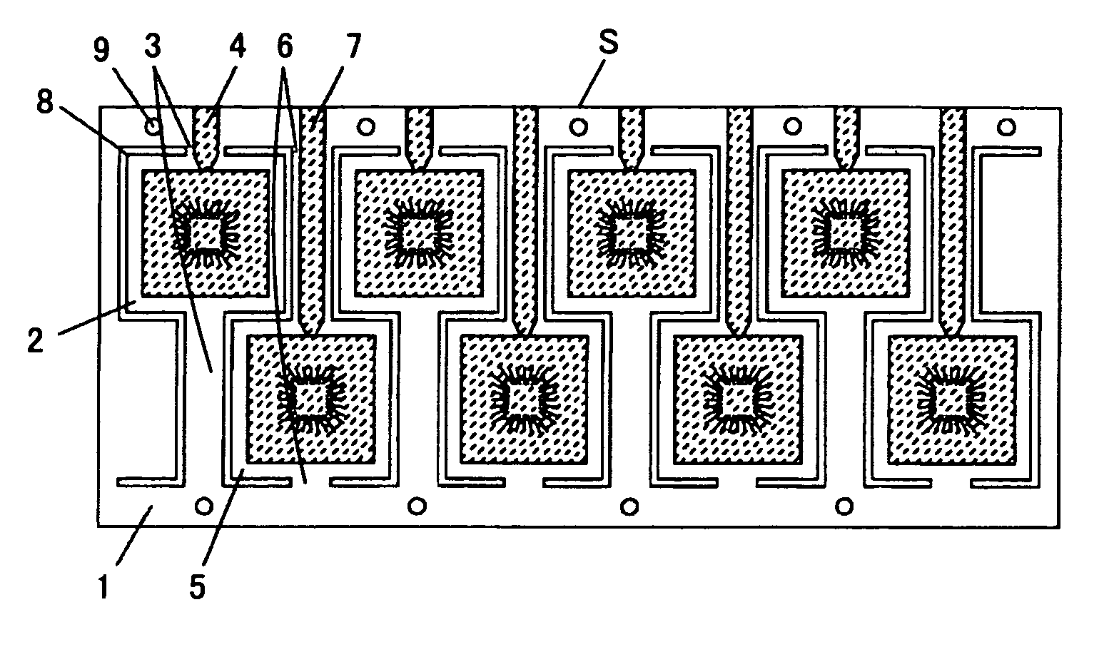
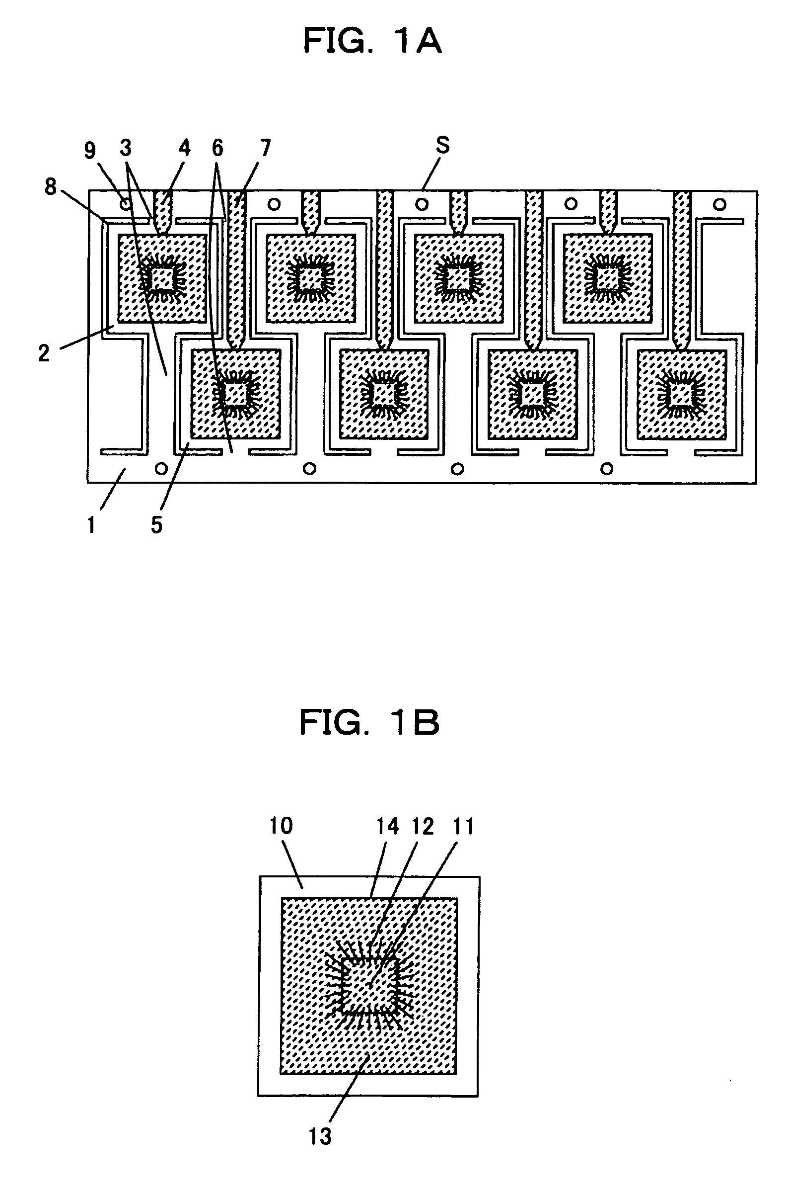
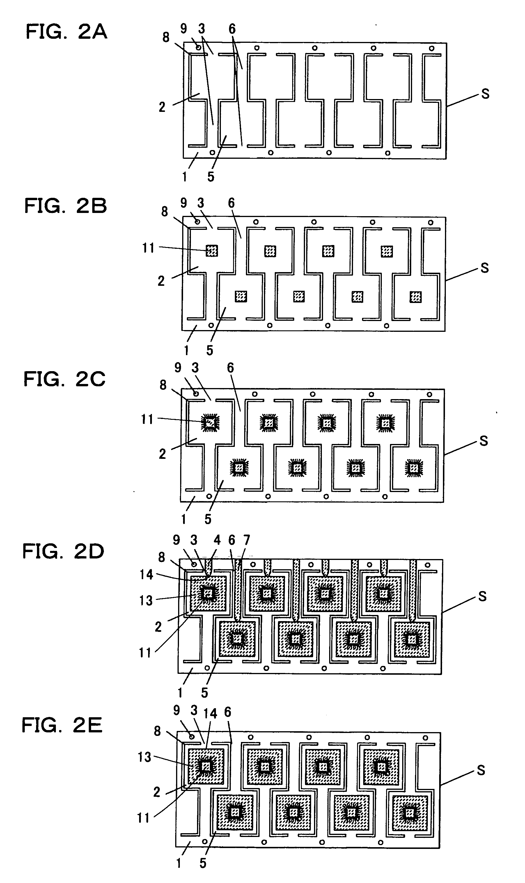
[0072]FIG. 1A shows an encapsulated state of a BGA package according to a first embodiment of the present invention. FIG. 1B shows a divided BGA package. FIGS. 2A to 2E show a process of manufacturing the BGA package using a semiconductor mount substrate according to the first embodiment of the present invention.
[0073] In FIGS. 1 and 2A to 2E, reference character S denotes a semiconductor mount substrate, reference numeral 1 a frame (connecting portion), reference numeral 2 a segment in a front row (a region divided in correspondence with each package), reference numeral 3 front-row tie bars, reference numeral 4 a runner to the front row, reference numeral 5 a segment in a rear row (a region divided in correspondence with each package), reference numeral 6 rear-row tie bars, reference numeral 7 a runner to the rear row, reference numeral 8 an opening, reference numeral 9 a positioning pin hole, reference numeral 10 a divided BGA package, reference numeral 11 a chip (semiconductor d...
second embodiment
[0087]FIG. 3 shows an encapsulated state of a BGA package on a semiconductor mount substrate S in a second embodiment of the present invention. Referring to FIG. 3, the semiconductor mount substrate S is the same as that shown in FIG. 2A. The peripheral sides of segments 2 and 5 are formed parallel to the substrate peripheral edges of the frame 1. Chips 11 are mounted on the semiconductor mount areas of the segments 2 and 5, and resin encapsulated portions 13 in which the chips 11 are encapsulated are formed on the segments 2 and 5.
[0088] The sides of the external shape of each resin encapsulated portion 13 are inclined through 45 degrees from the peripheral sides of the segment 2 or 5. Each gate 14 is positioned at a center of one peripheral side of the segment 2 or 5 and at an apex of the resin encapsulated portion 13.
[0089] The above-described construction ensures that, at the time of gate break, i.e., when the runners 4 and 7 are cut off from the segments 2 and 5 and the resin...
third embodiment
[0094]FIG. 4 shows an encapsulated state of a BGA package on a semiconductor mount substrate S in a third embodiment of the present invention. Referring to FIG. 4, the semiconductor mount substrate S is basically the same as that shown in FIG. 2A. A point of difference therefrom is as described below.
[0095] That is, each of segments 2 and 5 has such a shape that its peripheral sides are inclined through 45 degrees from the substrate peripheral edges of the frame 1. On the segments 2 and 5 are formed resin encapsulated portions 13 in which chips 11 are encapsulated while being mounted on the semiconductor mount areas of the segments 2, as are those in the above-described embodiments.
[0096] The sides of the external shape of each resin encapsulated portion 13 are inclined through 45 degrees from the substrate peripheral edges of the frame 1 and are parallel to the peripheral sides of the segment 2 or 5. Each gate 14 is positioned at one apex of the segment 2 or 5 and at one apex of ...
PUM
| Property | Measurement | Unit |
|---|---|---|
| Angle | aaaaa | aaaaa |
| Shape | aaaaa | aaaaa |
| Width | aaaaa | aaaaa |
Abstract
Description
Claims
Application Information