High integrated semiconductor memory device

a memory device and semiconductor technology, applied in the field of high integrated semiconductor memory devices, to achieve the effect of reducing the layout size of the semiconductor memory devices

Active Publication Date: 2007-04-26
SK HYNIX INC
View PDF2 Cites 11 Cited by
  • Summary
  • Abstract
  • Description
  • Claims
  • Application Information

AI Technical Summary

Benefits of technology

[0014] It is an object of the present invention to provide a semiconductor memory device having a 6F2 open bit line structure which connects each of a bit line pair to each of a neighboring bit line pair for a precharge operation so that a layout size of the semiconductor memory device decreases.

Problems solved by technology

At issue for higher integration is how to make a minuter pattern in the semiconductor memory device.

Method used


Image

  • High integrated semiconductor memory device
  • High integrated semiconductor memory device
  • High integrated semiconductor memory device

Examples


Embodiment Construction

[0021] Hereinafter, a semiconductor memory device in accordance with specific embodiments of the present invention will be described in detail with reference to the accompanying drawings.

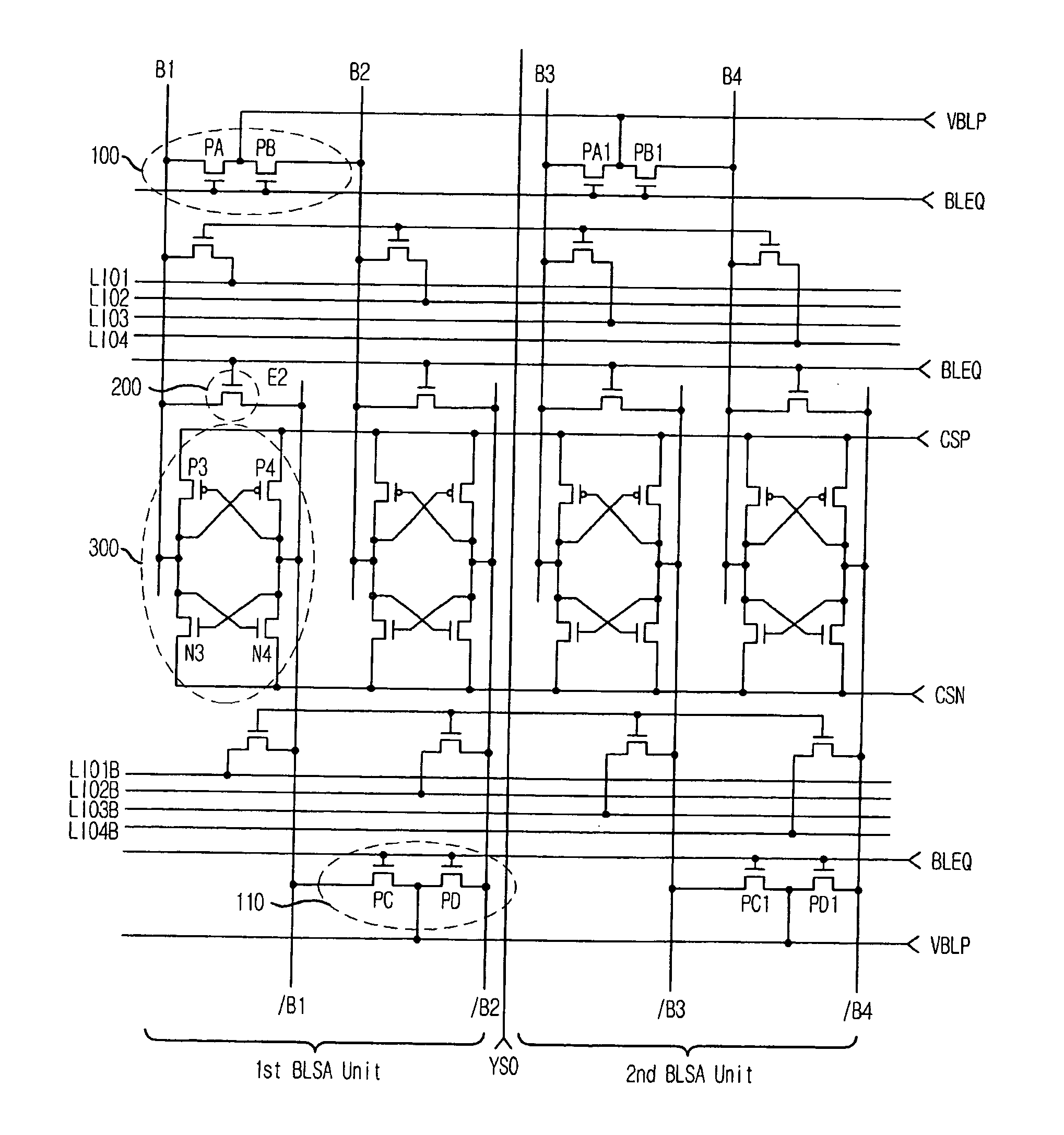
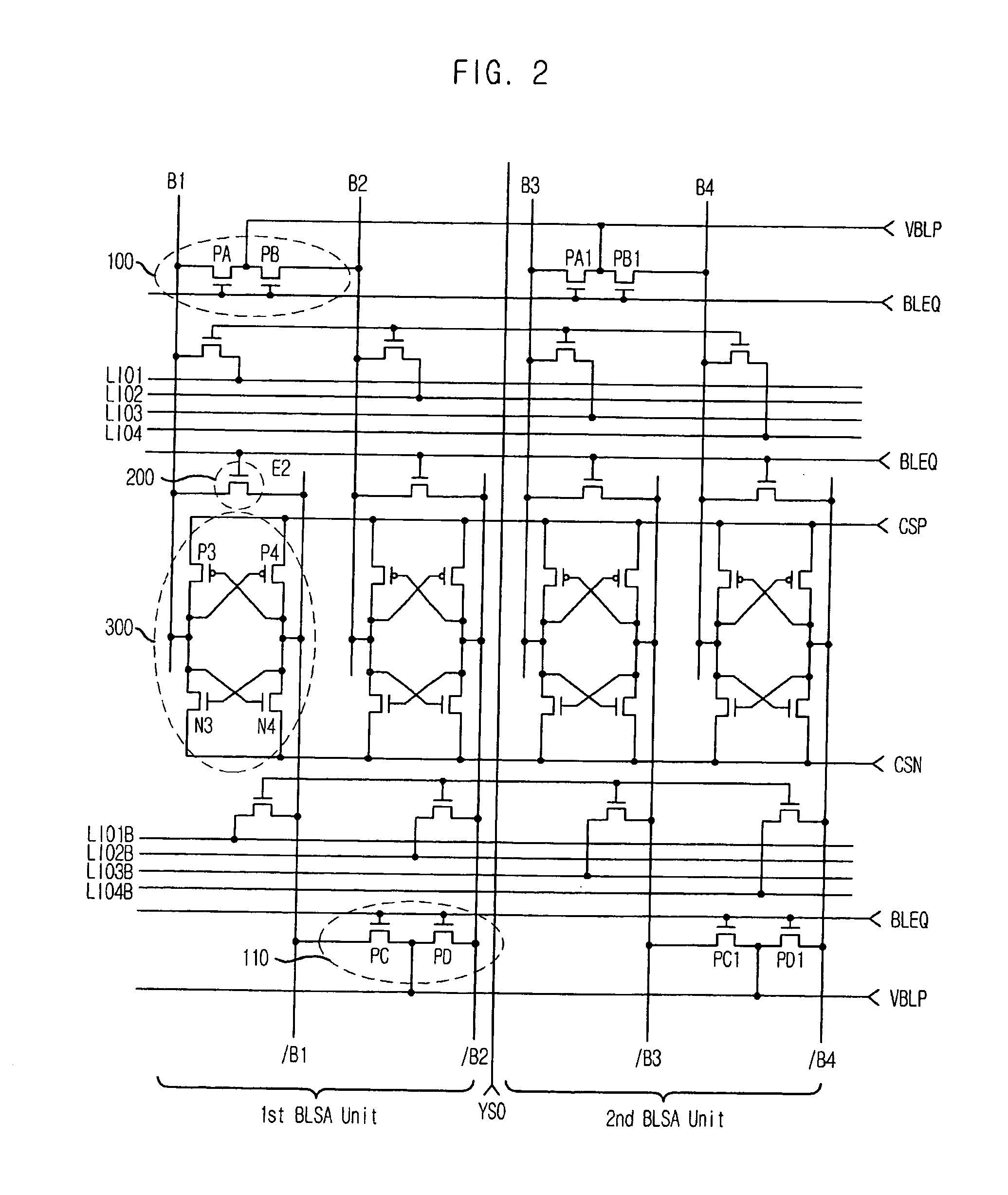
[0022]FIG. 2 is a schematic circuit diagram of a sense amplifying block included in a semiconductor memory device in accordance with the present invention.

[0023] The sense amplifying block includes first and second precharge units 100 and 110, an equalizing unit 200, and a sense amplifier 300.

[0024] The first precharge unit 100 precharges one of a first bit line pair B1 and / B1 and one of a second bit line pair B2 and / B2 in response to a bit line equalizing signal VBLP. The second precharge unit 110 precharges the other of the first bit line pair B1 and / B1 and the other of the second bit line pair B2 and / B2 in response to the bit line equalizing signal VBLP. Particularly, in FIG. 2, the first precharge unit 100 precharges a first bit line B1 and a second bit line B2 and the second precharge un...


PUM


Abstract

A semiconductor memory device, having a 6F2 open bit line structure, connects each bit line of a bit line pair to a respective bit line of a neighboring bit line pair for a precharge operation so that a layout size of the semiconductor memory device decreases. Plural first precharge units each precharge one bit line of a first bit line pair and one bit line of a second bit line pair in response to a bit line equalizing signal. Plural sense amplifiers each sense a data bit supplied to a respective one of the first and second bit line pairs and amplify sensed data.

Description

FIELD OF INVENTION [0001] The present invention relates to a semiconductor memory device; and, more particularly, to a high integrated sense amplifier of which layout size can be reduced in a semiconductor memory device having an open bit line structure. DESCRIPTION OF RELATED ARTS [0002] Integration and capability of a semiconductor memory device is continuously being enhanced. There are two issues that are primarily addressed: increasing the speed at which the semiconductor memory device can operate, and increasing data storage capability of the semiconductor memory device in a restricted area. [0003] As storage capacity of the semiconductor memory device increases, a larger area is required and / or higher integration. At issue for higher integration is how to make a minuter pattern in the semiconductor memory device. A fold bit line structure (generally, referred as to an 8F2 cell structure) and an open bit line structure (generally, referred as to a 6F2 cell structure) have been ...

Claims


Application Information

Patent Timeline
Patent Type & Authority Applications(United States)
IPC IPC(8): G11C11/34
CPCG11C7/12G11C7/18G11C11/419G11C7/06
Inventor WON, HYUNG-SIK
Owner SK HYNIX INC
Why Eureka
Try Eureka