Bit error rate based system and method for optimizing communication system performance

a communication system and error rate technology, applied in the direction of error prevention, digital transmission, transmission monitoring, etc., can solve the problems of bit error rate and inability to adapt to module components, and achieve the effect of reducing data transmission errors

Inactive Publication Date: 2007-04-26
AVAGO TECH WIRELESS IP SINGAPORE PTE
View PDF7 Cites 6 Cited by
  • Summary
  • Abstract
  • Description
  • Claims
  • Application Information

AI Technical Summary

Benefits of technology

[0016] By using the foregoing techniques, data errors may be reduced with a degree of speed and accuracy previously unavailable.

Problems solved by technology

However, such modules have not permitted adaptive alteration of module components to reduce the bit error rate.

Method used


Image

  • Bit error rate based system and method for optimizing communication system performance
  • Bit error rate based system and method for optimizing communication system performance
  • Bit error rate based system and method for optimizing communication system performance

Examples


Embodiment Construction

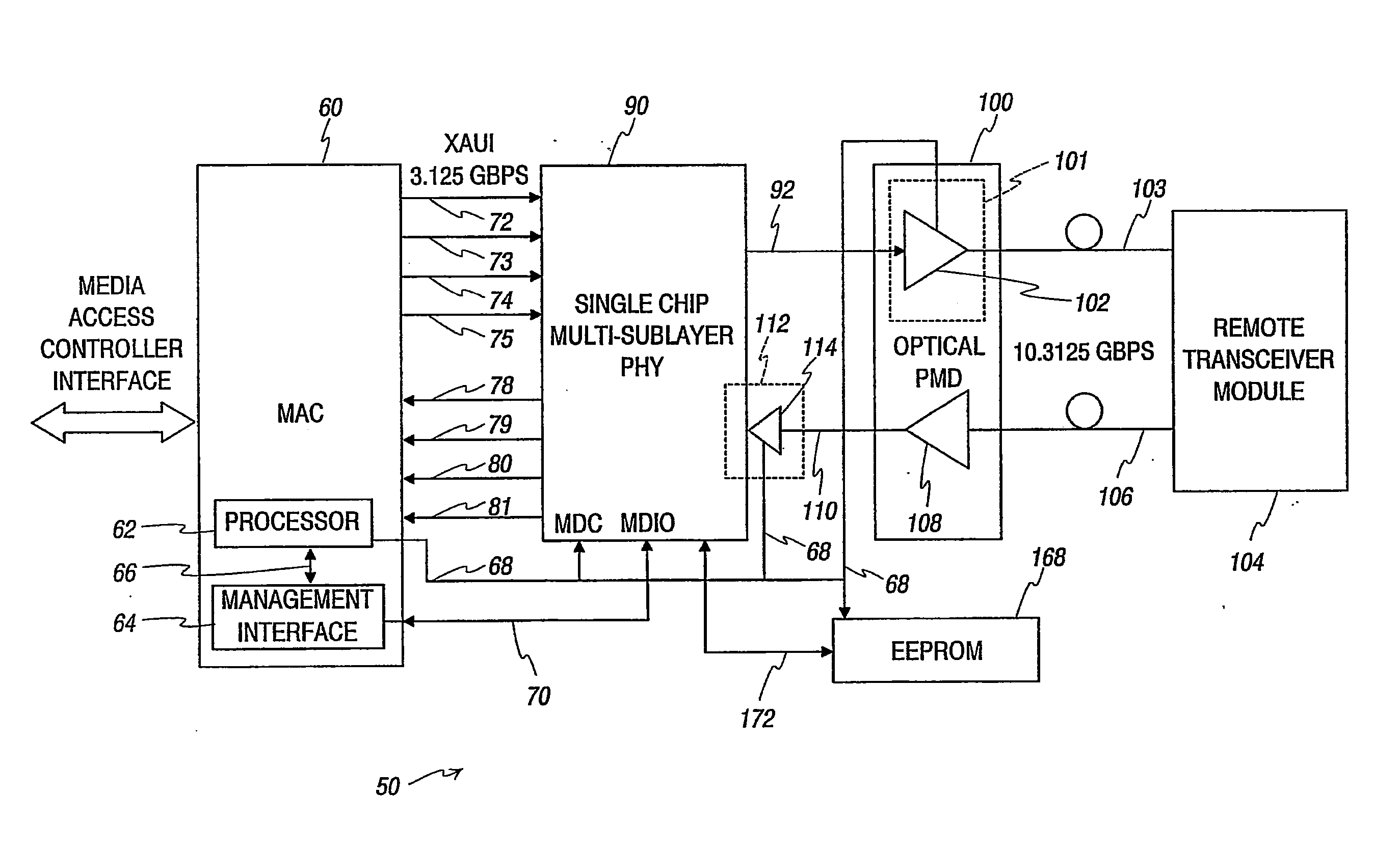
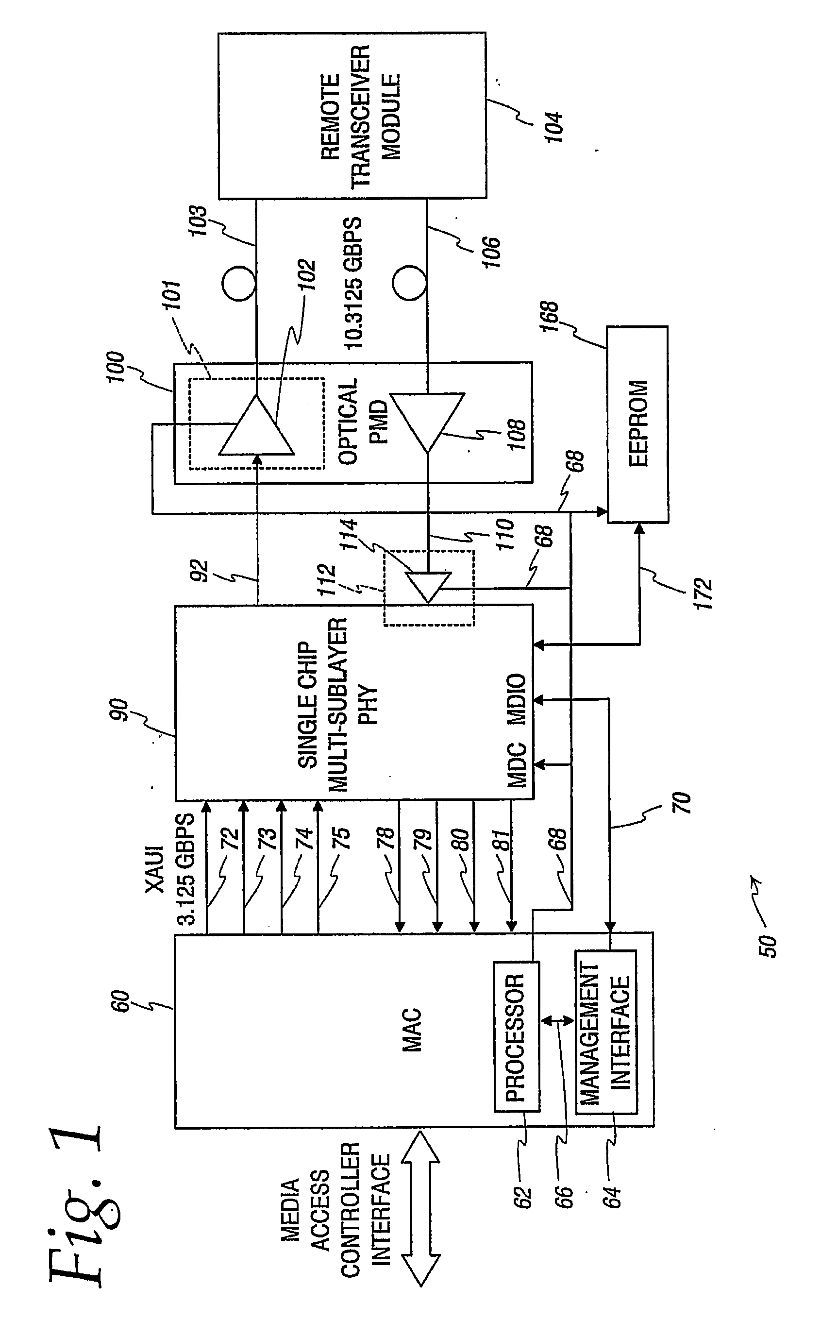
[0023] Referring to FIG. 1, a system 50 for transmitting data on a network and receiving data from the network made in accordance with one embodiment of the invention includes a media access controller (MAC) 60, which includes a processor or controller 62. The processor 62 communicates with a management interface 64 over a bus 66 and communicates with a control bus 68 that transmits control signals generated by processor 62. The control signals are generated according to an error correction algorithm in response to error signals received by interface 64 over an input / output bus 70. Module 60 transmits data at about 3.125 Giga bits per second (Gbps) on each of paths 72-75, and module 60 receives data at about 3.125 Gbps on each of paths 78-81.

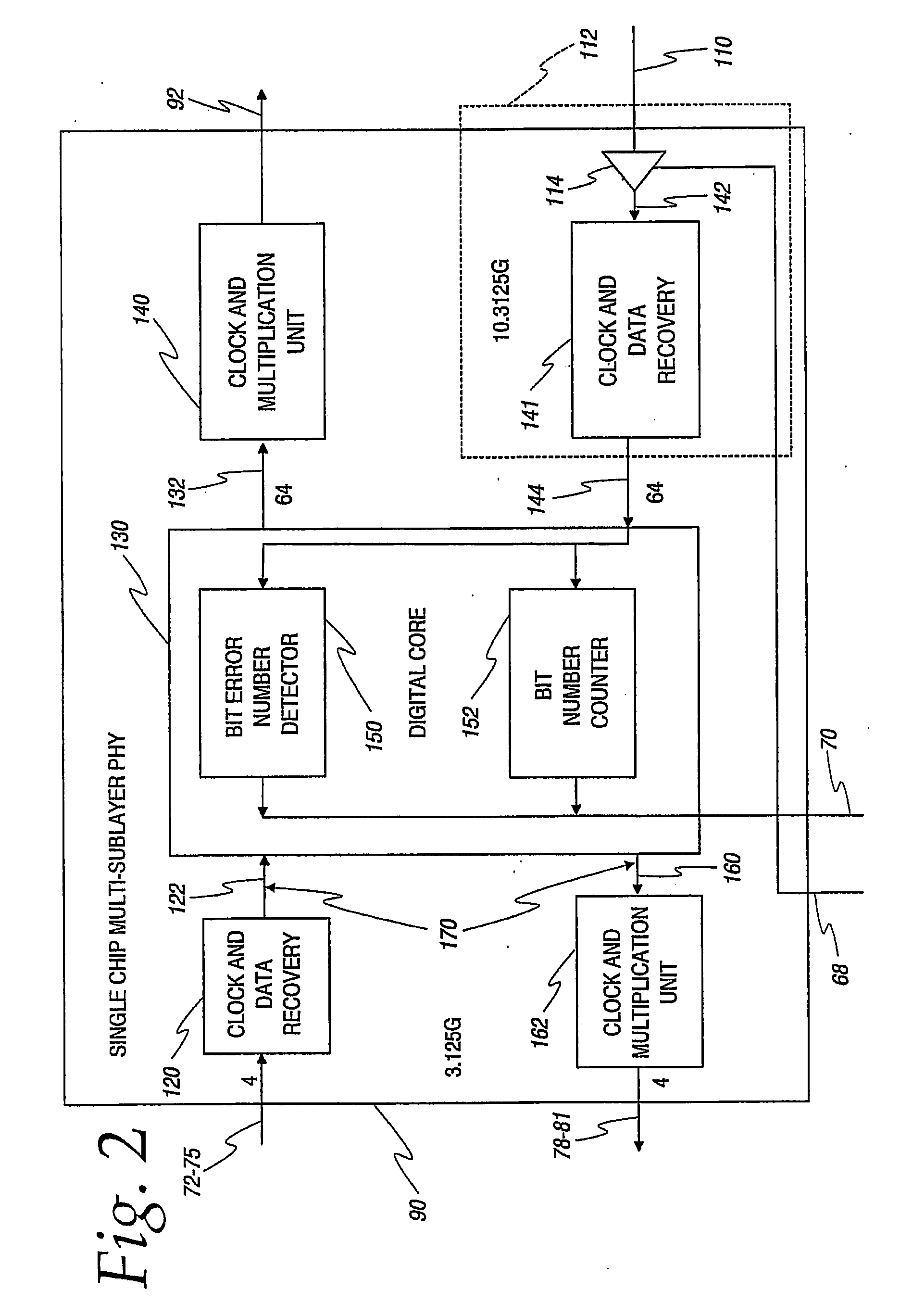
[0024] A single chip multi-sublayer PHY 90 includes modules for converting the 3.125 input parallel data on paths 72-75 to serial 10.3125 Gbps electrical output data on a path 92. The output data is converted to optical data by a conversion mod...


PUM


Abstract

A system (50) includes a communication path (170) and transmits data on a network (103, 106). A transmitter (101) transmits data on the network and a receiver (112) receives data from the network. A component (102, 114) in the communication path has a transfer characteristic (C1, C2, C3) adjusted in response to errors in data transmitted over and received from the network in order to reduce the error rate.

Description

CROSS-REFERENCE TO RELATED APPLICATIONS / INCORPORATION BY REFERENCE [0001] U.S. Pat. No. 6,424,194, U.S. application Ser. No. 09 / 540,243 filed on Mar. 31, 2000, U.S. Pat. No. 6,389,092, U.S. Pat. No. 6,340,899, U.S. application Ser. No. 09 / 919,636 filed on Jul. 31, 2001, U.S. application Ser. No. 09 / 860,284 filed on May 18, 2001, U.S. application Ser. No. 10 / 028,806 filed on Oct. 25, 2001, U.S. application Ser. No. 09 / 969,837 filed on Oct. 1, 2001, U.S. application Ser. No. 10 / 159,788 entitled “Phase Adjustment in High Speed CDR Using Current DAC” filed on May 30, 2002, U.S. application Ser. No. 10 / 179,735 entitled “Universal Single-Ended Parallel Bus; fka, Using 1.8V Power Supply in 0.13 MM CMOS” filed on Jun. 21, 2002, and U.S. application Ser. No. 60 / 402,097 entitled “SYSTEM AND METHOD FOR IMPLEMENTING A SINGLE CHIP HAVING A MULTIPLE SUB-LAYER PHY” filed on Aug. 7, 2002 with attorney docket # 1772-13906US01, are each incorporated herein by reference in their entirety. The applican...

Claims


Application Information

Patent Timeline
Patent Type & Authority Applications(United States)
IPC IPC(8): H04B10/00H04L1/00
CPCH04B10/07953H04B10/0799
Inventor FAN, NONGHOANG, TUANJIANG, HONGTAOJEN, KEH-CHEE
Owner AVAGO TECH WIRELESS IP SINGAPORE PTE
Why Eureka
Try Eureka