

Analog signal processing circuit for ccd camera, and analog signal processing method
- Summary
- Abstract
- Description
- Claims
- Application Information
AI Technical Summary
Benefits of technology
Problems solved by technology
Method used
Image

Examples
first embodiment
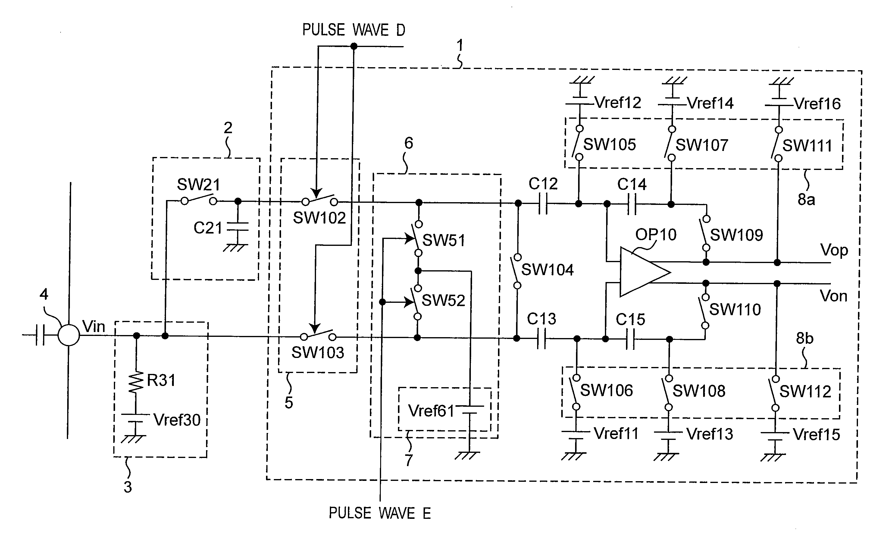
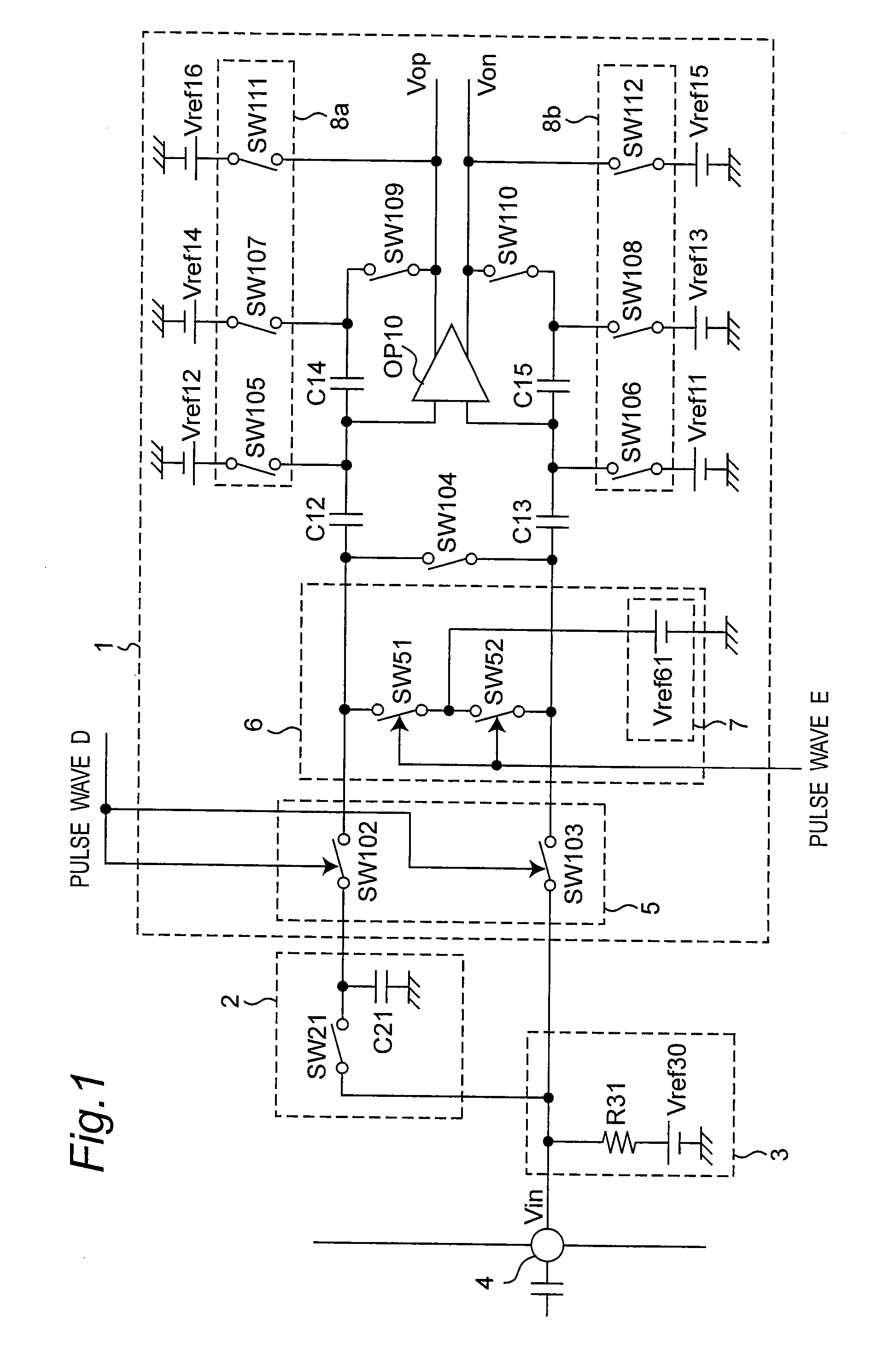
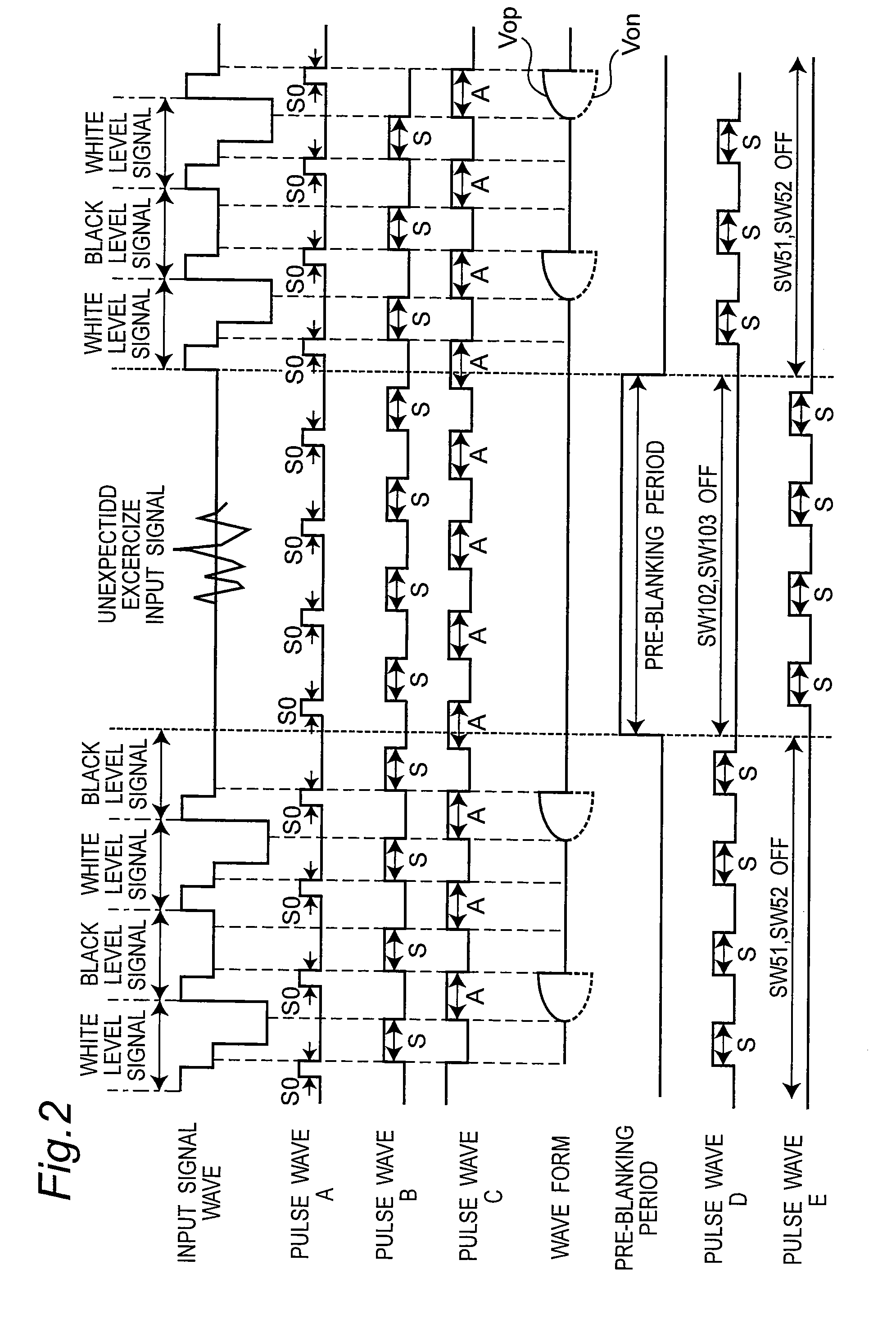
[0025]FIG. 1 is a circuit diagram showing a configuration of an analog signal processing circuit for a CCD camera according to a first embodiment of the present invention. The analog signal processing circuit for a CCD camera includes a switched capacitor amplification circuit 1, a black level sample / hold circuit 2 and an input DC level circuit 3.
[0026] As illustrated in FIG. 1, the switched capacitor amplification circuit 1 includes an operational amplification circuit OP10, a first switch circuit section 5 (SW102, SW103), sampling switch circuit sections 8a and 8b (SW105 to SW108, SW111, SW112), amplifying switch circuits SW104, SW109 and SW110, capacitors C12 to C15, bias circuits Vref11 to Vref16, a second switch circuit section 6 having switch circuits SW51 and SW52, and a bias circuit section 7 having a bias circuit Vref61. Herein, the switch circuits SW51 and SW52 in the second switch circuit section 6 and the bias circuit Vref61 in the bias circuit section 7 are newly provi...
PUM
 Abstract
Description
Claims
Application Information