Eureka AIR delivers breakthrough ideas for toughest innovation challenges, trusted by R&D personnel around the world.

Image data processing semiconductor integrated circuit

Inactive Publication Date: 2007-05-03
RENESAS TECH CORP
View PDF4 Cites 5 Cited by
  • Summary
  • Abstract
  • Description
  • Claims
  • Application Information

AI Technical Summary

Benefits of technology

[0007] The present invention has been made to address the above problems and its objects are to reduce the number of parts constituting an image capturing system using a solid-state image sensor and to reduce the size and cost of mobile electronic appliances including a camera function.
[0020] According to the present invention, it is possible to reduce the number of parts constituting an image capturing system using a solid-state image sensor and reduce the size and cost of a mobile electronic appliance having camera functionality.

Problems solved by technology

This would be a cause making it impossible to downsize appliances such as mobile phones incorporating an electronic cameral using the CCD sensor.
This poses further problems in which power consumption is further increased by driving the bus and the bus operation itself becomes a source of noise to the analog circuits.

Method used


Image

  • Image data processing semiconductor integrated circuit
  • Image data processing semiconductor integrated circuit
  • Image data processing semiconductor integrated circuit

Examples


first embodiment

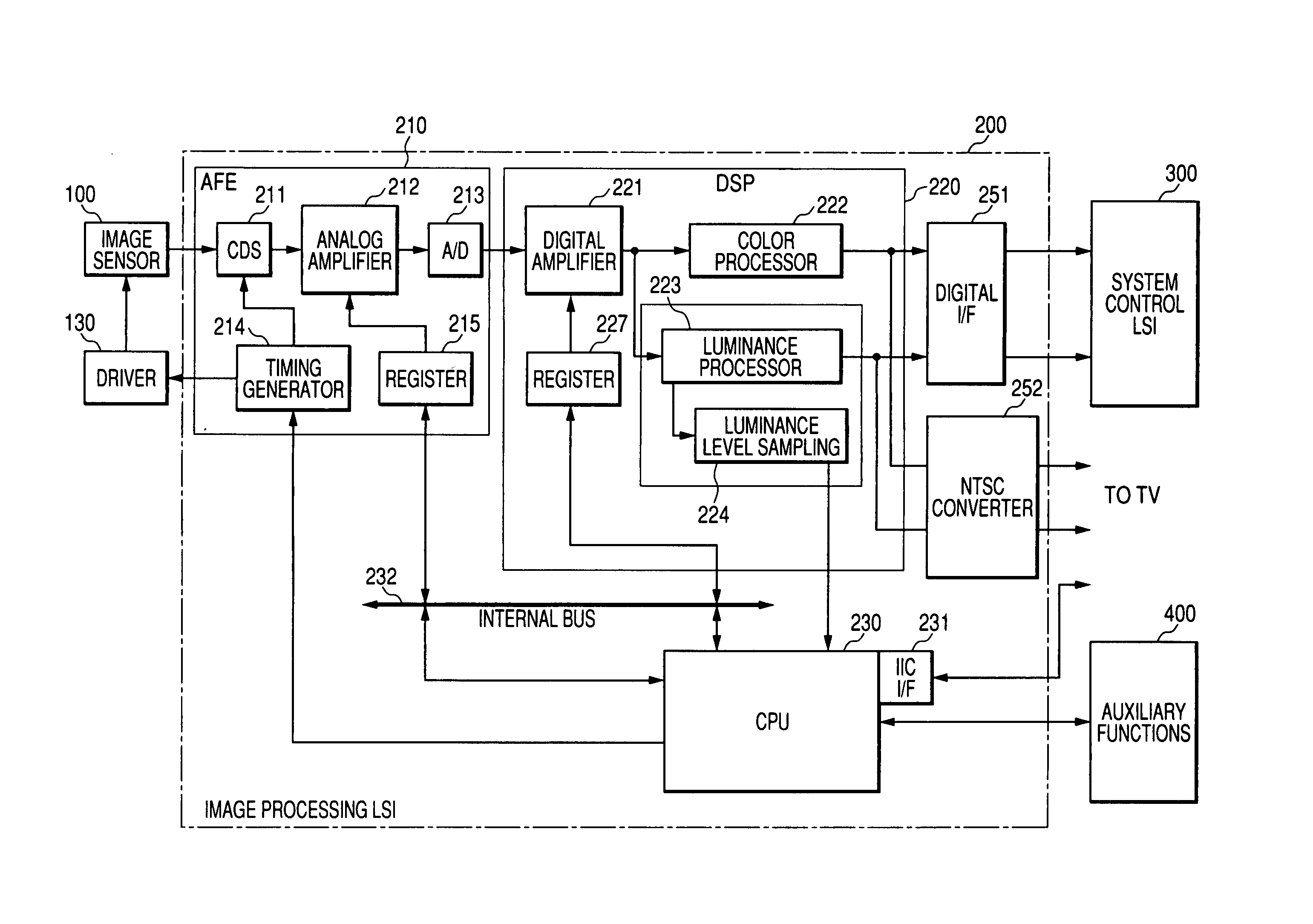
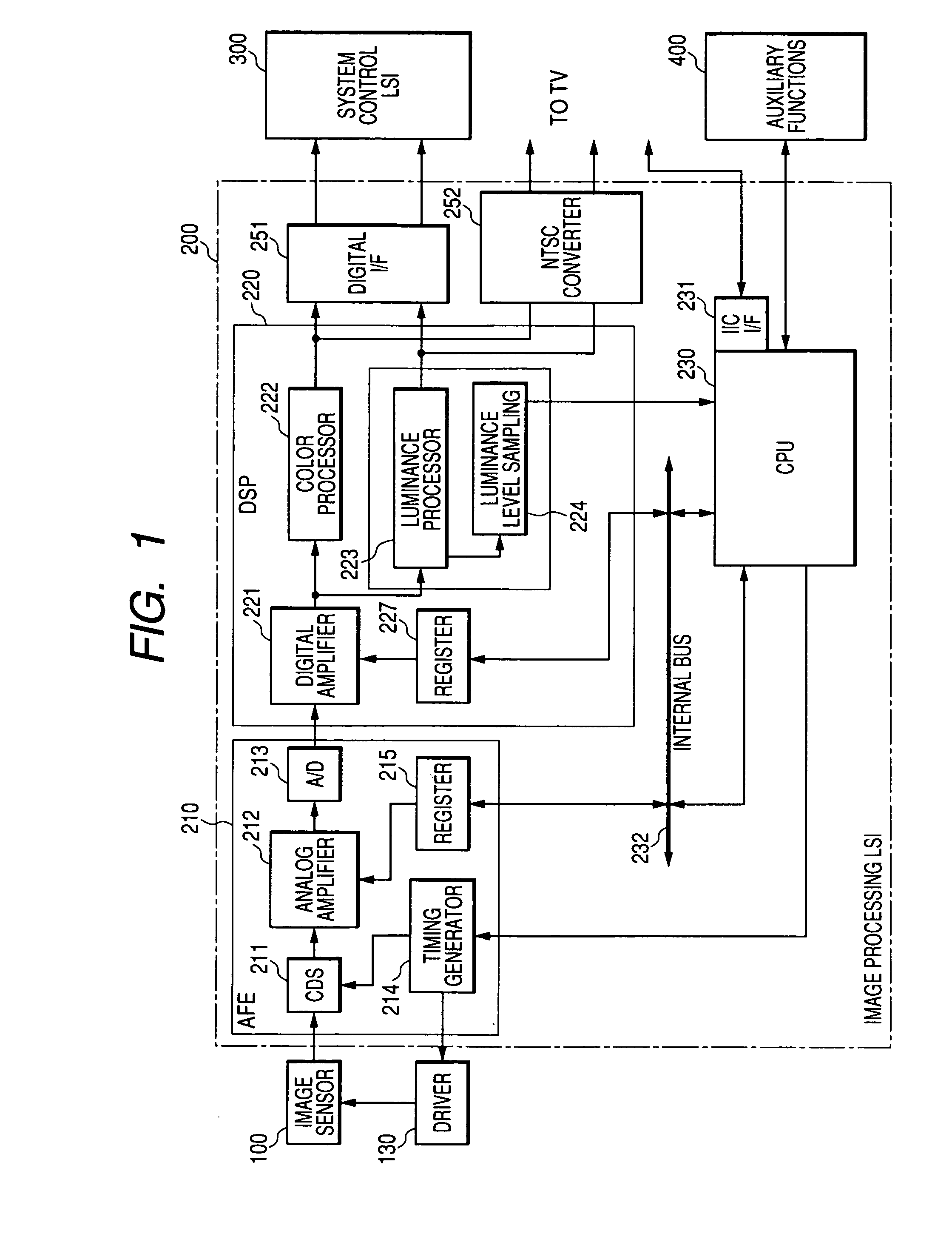
[0028]FIG. 1 shows a block diagram representing an image data processing semiconductor integrated circuit (hereinafter referred to as an image processing LSI) to which the present invention is applied and an example of an image capturing system configuration using this embodiment.

[0029] The image capturing system shown in FIG. 1 is constructed with a CCD type solid-state image sensor 100, an image processing LSI 200 including an AFE (analog front end) section 210, an image processor 220 which performs digital image processing, and a CPU 230 which performs overall control of the chip, register configuration, etc., a system control LSI 300, and a circuit of auxiliary functions 400 such as optical zooming.

[0030] When, for example, the applied system is a mobile phone, the system control LSI 300 is an electronic device including a microcomputer or the like, specifically, including a baseband LSI responsible for processing of voice signals and transmit / receive signals and an LSI having ...

second embodiment

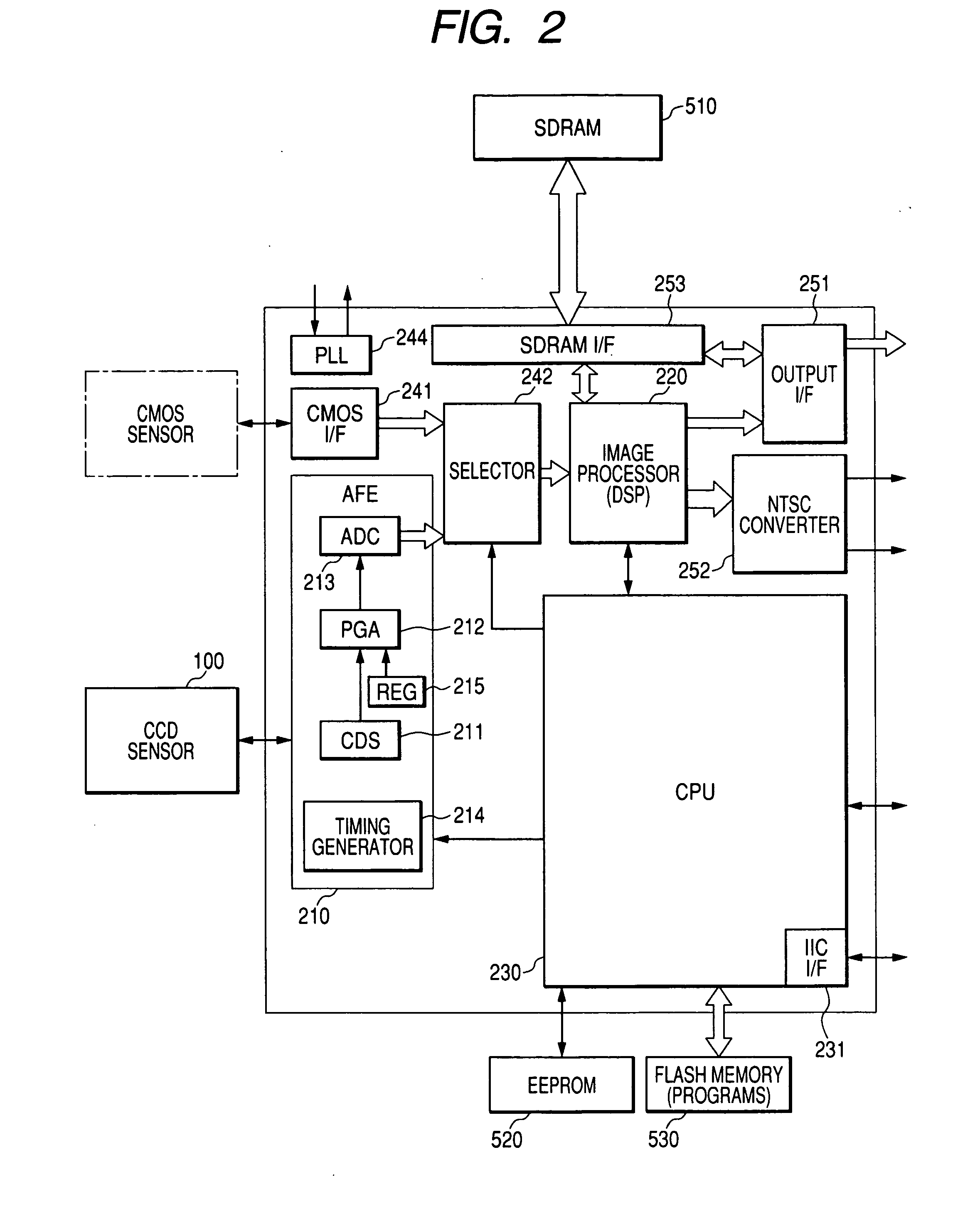
[0046]FIG. 2 shows a block diagram representing an image processing LSI to which the present invention is applied and an example of an image capturing system configuration using this embodiment. Circuits having the same functions as the corresponding ones in the image processing LSI of the first embodiment in FIG. 1 are assigned the same numbers and their explanation is not repeated.

[0047] The image processing LSI of the second embodiment is provided with a CMOS interface 241 which receives signals output from a CMOS sensor including the AFE functionality and outputs a control signal to the AFE in the CMOS sensor. This LSI is configured so as to be able to process both image signals from the CCD sensor and image signals from the CMOS sensor.

[0048] Accordingly, a selector 242 is provided which selects either type of the image signals input from the CMOS sensor via the CMOS interface 241 and the image signals input from the CCD sensor via the AFE circuit 210 and supplies the selected...


PUM


Abstract

The invention is intended to reduce the number of parts constituting an image capturing system using a solid-state image sensor and reduce the size and cost of a mobile electronic appliance having camera functionality. An analog front end circuit for an image capturing system, which samples pixel readout signals input from a solid-state image sensor, amplifies the sampled signals up to a predetermined level, and converts the amplified signals into digital signals, is formed, together with a DSP for digital image processing and a CPU responsible for arithmetic processing and control for camera functionality such as auto focusing and register setting, in a semiconductor integrated circuit on a single semiconductor chip.

Description

CROSS-REFERENCE TO RELATED APPLICATION [0001] The present application claims priority from Japanese application No. 2005-315693 filed on Oct. 31, 2005, the content of which is hereby incorporated by reference into this application. BACKGROUND OF THE INVENTION [0002] The present invention relates to an image processing technique for processing captured image signals output by a solid-state image sensor. In particular, the invention relates to a technique that is effectively used for an image data processing semiconductor integrated circuit which processes analog captured image signals output by a solid-state image sensor. [0003] As image sensors in video cameras and still cameras, a CCD type solid-state image sensor and a CMOS type solid-state image sensor are available. For the former CCD type solid-state image sensor, after parallel transfer of stored charges per pixel obtained by photoelectric conversion of incident light to a transfer CCD, the charges are serially transferred wit...

Claims


Application Information

Patent Timeline
IPC IPC(8): H04N5/228H04N5/225H04N5/335H04N5/341H04N5/376H04N5/378
CPCH04N5/2258H04N5/335H04N23/45H04N25/00
Inventor SHIDA, KOJISUZUKI, JUNKATO, YOICHIYAMADA, HIDEHITONISHIZAWA, AKIHITO
Owner RENESAS TECH CORP
Why Eureka
Eureka Blog
Learn More