
Word Line Driver For DRAM Embedded In A Logic Process

a logic process and driver technology, applied in the field of dynamic random accessible memory (dram), can solve the problem that the scheme cannot be readily applied to general logic circuits

Active Publication Date: 2007-05-17
MOSYS INC
View PDF63 Cites 27 Cited by
  • Summary
  • Abstract
  • Description
  • Claims
  • Application Information

AI Technical Summary

Benefits of technology

"The present invention provides a word line driver circuit for accessing a memory cell embedded in a logic process. The circuit includes an output driver that applies a negative boosted voltage to the memory cell using a p-channel pass-gate transistor and a deep n-type well region. The negative boosted voltage is lower than the ground voltage by an amount equal to or greater than the threshold voltage of the p-channel pass-gate transistor. The circuit also includes a p-channel transistor and a deep n-type well region that apply a positive boosted voltage to the memory cell using a p-channel access transistor. The positive boosted voltage is greater than the positive supply voltage by an amount usually less than the sub-threshold voltage of the p-channel pass-gate transistor. The circuit can be used in either embodiment, and the conductivity types of the elements can be reversed. The technical effect of the invention is to provide a more efficient and reliable method for accessing memory cells in logic processes."

Problems solved by technology

First, there is only one insulating layer between the capacitor electrode and counter-electrode.
This scheme however cannot be readily applied to general logic circuits, as logic circuits, in general, are designed with the substrate grounded.

Method used


Image

  • Word Line Driver For DRAM Embedded In A Logic Process
  • Word Line Driver For DRAM Embedded In A Logic Process
  • Word Line Driver For DRAM Embedded In A Logic Process

Examples


Embodiment Construction

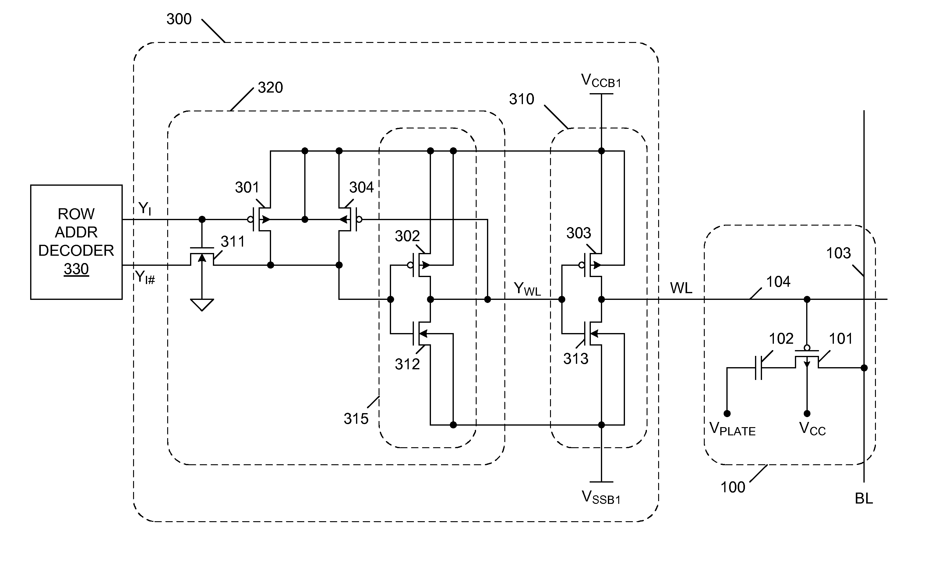
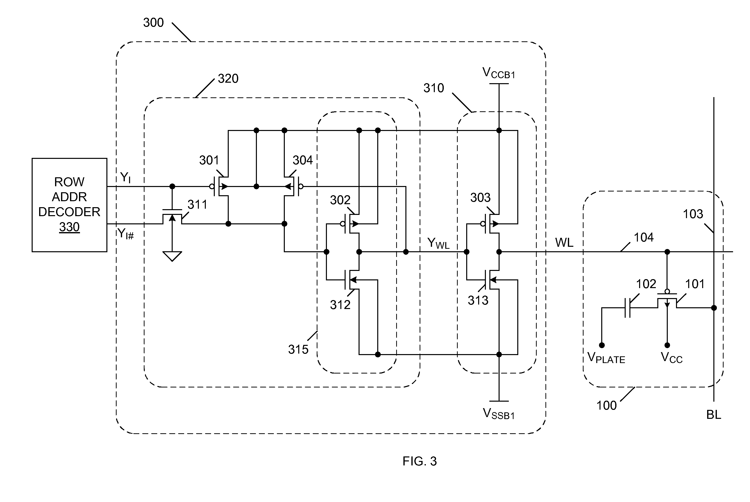
[0034]FIG. 3 is a circuit diagram of a word line driver 300 in accordance with one embodiment of the present invention. In this embodiment, word line driver 300 drives the word line 104 of embedded DRAM cell 100 (FIG. 1) in response to control signals YI and YI# provided by a row address decoder 330.

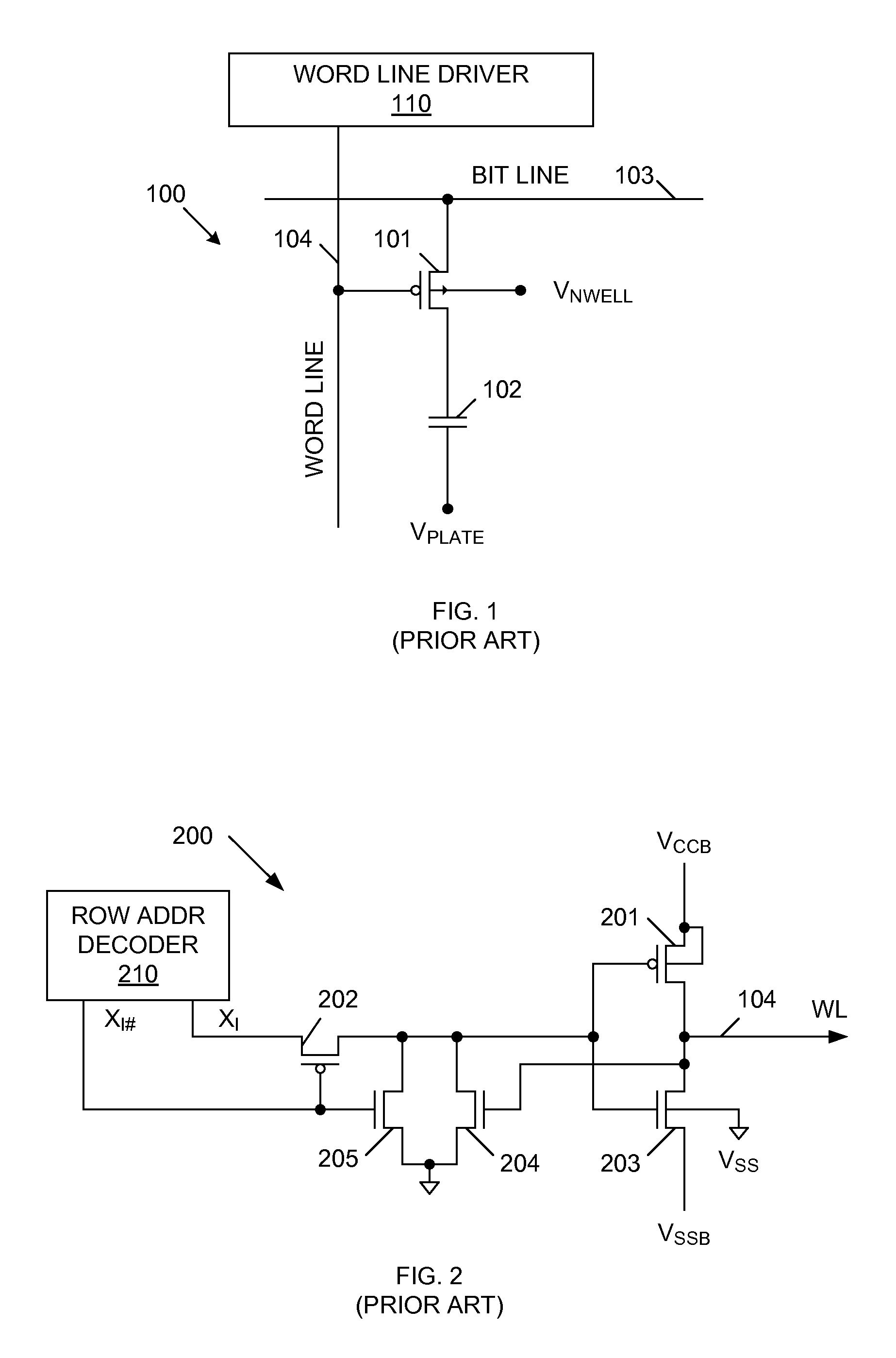
[0035] As described above in connection with FIG. 1, DRAM cell 100 is fabricated using a conventional logic process. DRAM cell 100 includes PMOS pass gate transistor 101 and cell capacitor 102. Cell capacitor 102 can be formed, for example, by a metal-insulator-metal (MIM) structure, as described in U.S. Patent Application Publication No. US2005 / 0082586 A1; a planar MOS device as described in U.S. Pat. No. 6,075,720; or a folded MOS device as described in U.S. Pat. No. 6,573,548 B2. Other capacitor structures compatible with a conventional logic process can be used to implement cell capacitor 102 in other embodiments.

[0036] As described above in connection with FIG. 1, DRAM cell 100 is...


PUM


Abstract

A word line driver is provided for accessing a DRAM cell embedded in a conventional logic process. The DRAM cell includes a p-channel access transistor coupled to a cell capacitor. The word line driver includes an n-channel transistor located in a p-well, wherein the p-well is located in a deep n-well. The deep n-well is located in a p-type substrate. A word line couples the drain of the n-channel transistor to the gate of the p-channel access transistor. A negative boosted voltage supply applies a negative boosted voltage to the p-well and the source of the n-channel transistor. The negative boosted voltage is less than ground by an amount equal to or greater than the threshold voltage of the p-channel access transistor. The deep n-well and the p-type substrate are coupled to ground. The various polarities can be reversed in another embodiment.

Description

RELATED APPLICATIONS [0001] The present application is a divisional of Ser. No. 11 / 166,856 filed Jun. 24, 2005.[0002] The present application is also related to U.S. Pat. No. 6,028,804 by Wingyu Leung, entitled “Method and Apparatus for 1-T SRAM Compatible Memory”; U.S. Pat. No. 6,573,548 B2 by Wingyu Leung and Fu-Chieh Hsu, entitled “DRAM cell Having a Capacitor Structure Fabricated Partially in a Cavity and Method for Operating the Same”; U.S. Pat. No. 6,147,914 by Wingyu Leung and Fu-Chieh Hsu, entitled “On-Chip Word Line Voltage Generation for DRAM Embedded in Logic Process”; and U.S. Pat. No. 6,075,720 by Wingyu Leung and Fu-Chieh Hsu, entitled “Memory Cell for DRAM Embedded in Logic”. These patents are hereby incorporated by reference in their entirety. [0003] 1. Field of the Invention [0004] The present invention is applicable to Dynamic Random Accessible Memory (DRAM). More particularly, this invention relates to DRAM fabricated using a logic compatible process. This inventi...

Claims


Application Information

Patent Timeline
Patent Type & Authority Applications(United States)
IPC IPC(8): G11C8/00
CPCG11C8/08G11C11/4085G11C2207/104H01L27/10897H10B12/50G11C11/4063G11C11/4074
Inventor LEUNG, WINGYU
Owner MOSYS INC
Learn More