Offset compensation device

a compensation device and offset compensation technology, applied in the field of electronic devices, can solve the problem of containing components of useless carrier signals, and achieve the effect of stably and accurately suppressing

Inactive Publication Date: 2007-05-17
FUJITSU LTD
View PDF6 Cites 8 Cited by
  • Summary
  • Abstract
  • Description
  • Claims
  • Application Information

AI Technical Summary

Benefits of technology

[0131] Therefore, the imbalance of the quadrature modulator is stably and accuratel

Problems solved by technology

As a result, the components of the useless carrier sig

Method used


Image

  • Offset compensation device
  • Offset compensation device
  • Offset compensation device

Examples


first embodiment

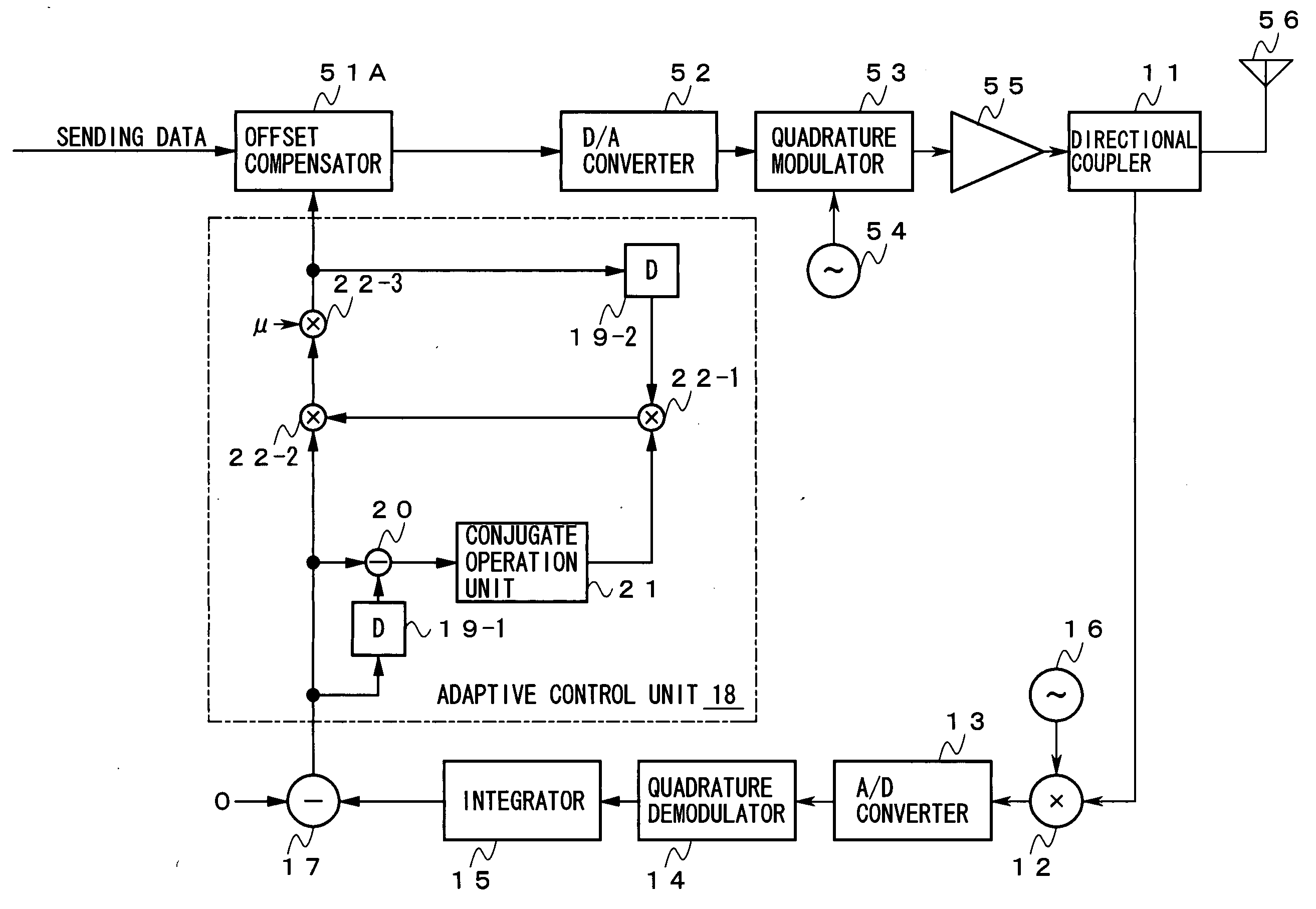
[0156]FIG. 1 is a block diagram showing the first embodiment of the invention.

[0157] This embodiment is provided with the following components:

[0158] an offset compensator 51A provided in place of the aforementioned offset compensator 51;

[0159] a directional coupler 11 arranged in the feeding path of an antenna 56;

[0160] a mixer 12, an A / D converter 13, a quadrature demodulator 14 and an integrator 15 cascaded with the monitor terminal of the directional coupler 11;

[0161] an oscillator 16 having an output connected with the local-frequency input of the mixer 12;

[0162] a subtracter 17 having its one input connected with the output of the integrator 15 and its other input set to “0” or the target value of the offset component to be compensated; and

[0163] an adaptive control unit 18 cascaded with the output of the subtracter 17 and having an output connected with the control input of the offset compensator 51A.

[0164] On the other hand, the adaptive control unit 18 is composed o...

second embodiment

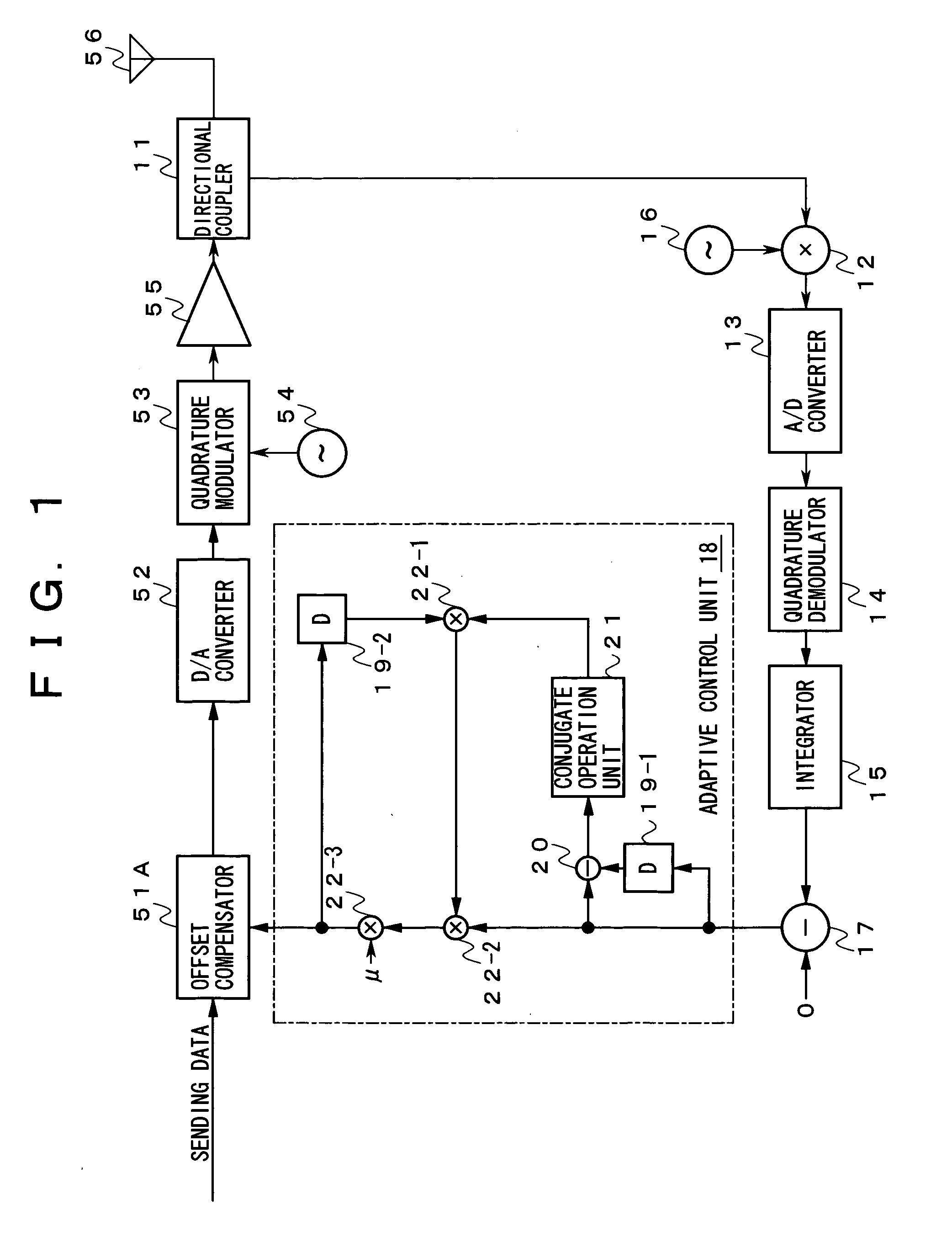
[0189]FIG. 3 shows the second embodiment of the present invention.

[0190] This embodiment is provided with the following components:

[0191] a phase operation unit 23 having its one input given the aforementioned sending data and its other input connected with the output of the quadrature demodulator 14; and

[0192] an adaptive control unit 18A connected with the output of the phase operation unit 23 and provided in place of the aforementioned adaptive control unit 18.

[0193] The adaptive control unit 18A is configured to have the following components:

[0194] a multiplier 24-1 having its one input connected with the output of the subtracter 17 and its other input connected with the output of the aforementioned phase operation unit 23; and

[0195] a multiplier 24-2 having its one input connected with the output of the multiplier 24-1 and its other input fed with the aforementioned step size μ and having its output connected with the control input of the offset compensator 51A.

[0196] Th...

third embodiment

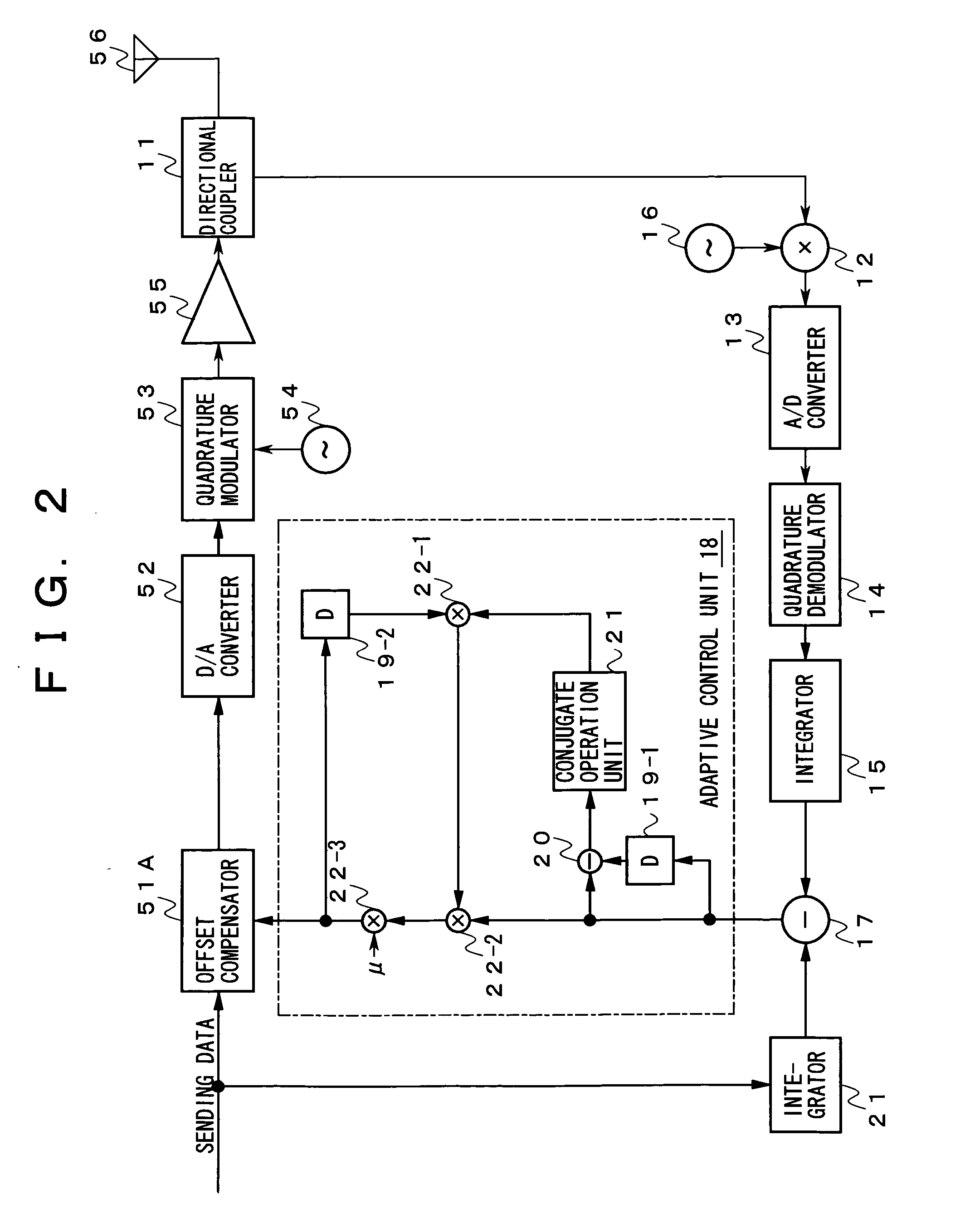
[0201]FIG. 4 is a block diagram showing the third embodiment of the present invention.

[0202] This embodiment is configured to include an adaptive control unit 18B characterized to have the following components, in place of the aforementioned adaptive control unit 18:

[0203] an absolute value calculation unit (ABS) 25 having its input connected with the output of the conjugate operation unit 21;

[0204] a multiplier 22-4 having its one input connected with the output of the absolute value calculation unit 25 and its other input connected with the output of the aforementioned multiplier 22-1;

[0205] an adder 26 having one its one input connected with the output of the multiplier 22-4;

[0206] a delayer (D) 27 having its input connected with the output of the adder 26 and its output connected with the other input of the adder 26;

[0207] a normalizing unit 28 having its input connected with the output of the adder 26: and

[0208] a multiplier 22-5 having its one input connected with the o...


PUM


Abstract

In an electronic device having a circuit outputting a vector sum of two quadrature vector signals, an offset compensating device compensates the offset contained in the vector sum. The offset compensating device aims to flexibly adapt to deviation in characteristics and performances and various fluctuations, and to compensate offset stably and accurately. The offset compensating device includes a deviation monitor unit creating a vector signal by A/D-converting the aforementioned vector sum and by quadrature-demodulating it and monitoring the deviation of the DC components superposed on the vector signal, and an adaptive control unit updating the compensation vector determined in advance, based on adaptive algorithm minimizing expectation value of the product of the inner product between an increment vector and the compensation vector, and the latest deviation vector, and adding the compensation vector to an offset vector to be inputted, while being superposed on the input signal, to a circuit.

Description

CROSS REFERENCE TO RELATED APPLICATION [0001] This application is a continuation of International Application PCT / JP2004 / 004647, filed Mar. 31, 2004, and designating the U.S., which is based upon and claims the benefit of priority from International Patent Application PCT / JP2003 / 11364, filed Sep. 5, 2003, the entire contents of which are herein incorporated by reference.BACKGROUND OF THE INVENTION [0002] 1. Field of the Invention [0003] The present invention relates to an electronic device which is provided with a circuit for processing two quadrature AC signals by predetermined operations in response to an input signal thereby to output a vector sum of the operations and, more particularly, to an offset compensation device for compensating the offset which is caused in the vector sum due to the change in the characteristics and the deviation of analog circuits for the individual operations. [0004] 2. Description of the Related Art [0005] The quadrature modulator for generating a mo...

Claims


Application Information

Patent Timeline
IPC IPC(8): H04L25/49H03C3/40H04L27/00H04L27/36
CPCH03C3/406H04L27/364H04L2027/0016H04L2027/0018H04L2027/0067H04L2027/0069
Inventor NAGATANI, KAZUOISHIKAWA, HIROYOSHIFUDABA, NOBUKAZUKUBO, TOKURO
Owner FUJITSU LTD
Why Eureka
Try Eureka