Semiconductor package and method of fabricating the same

Active Publication Date: 2007-05-24
SEMICON COMPONENTS IND LLC
View PDF40 Cites 21 Cited by
  • Summary
  • Abstract
  • Description
  • Claims
  • Application Information

AI Technical Summary

Benefits of technology

[0009] The present invention provides a semiconductor package which is small in size but inclu

Problems solved by technology

However, a decrease in the number of pads of each semiconductor chip requires an increase in the number of terminals of the CSP.
Hence, it is difficult to form an increased number of terminals spaced from each other at a predetermined pitch on a small semiconductor chip.
However, a meth

Method used


Image

  • Semiconductor package and method of fabricating the same
  • Semiconductor package and method of fabricating the same
  • Semiconductor package and method of fabricating the same

Examples


Example

[0024] The present invention will now be described more fully with reference to the accompanying drawings, in which exemplary embodiments of the invention are shown. The invention may, however, be embodied in many different forms and should not be construed as being limited to the embodiments set forth herein; rather, these embodiments are provided so that this disclosure will be thorough and complete, and will fully convey the concept of the invention to those skilled in the art. In the drawings, the thicknesses of layers and regions are exaggerated for clarity.

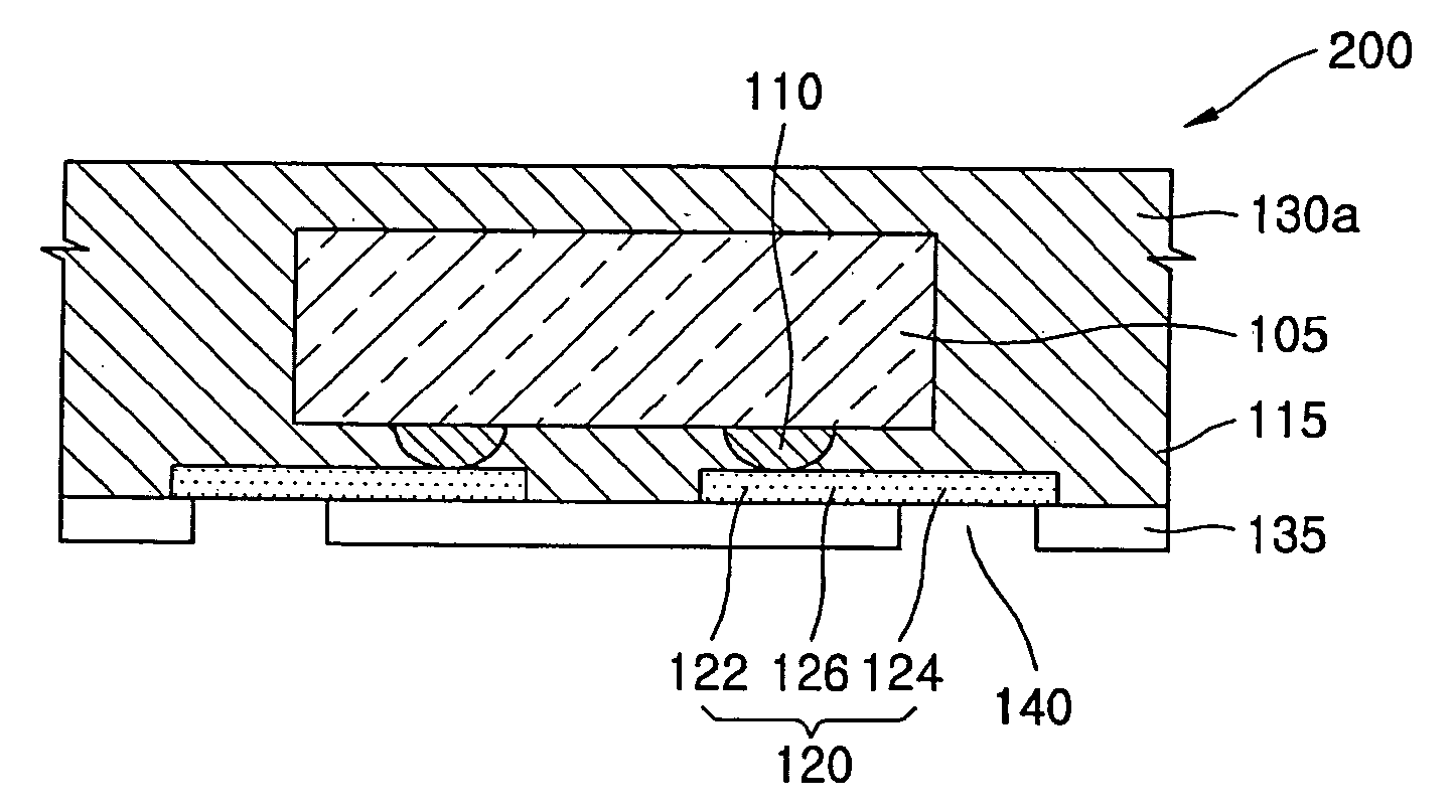
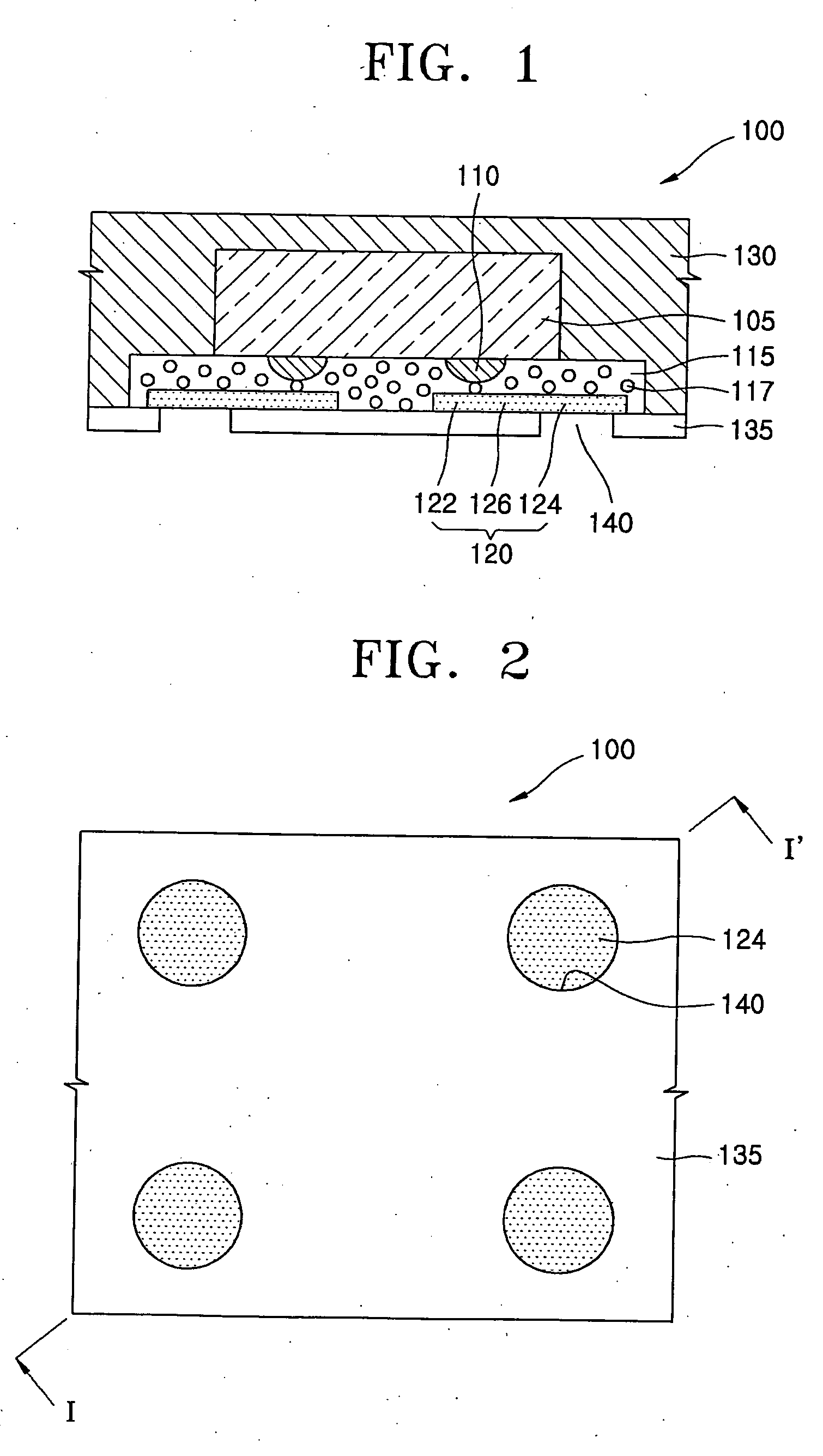
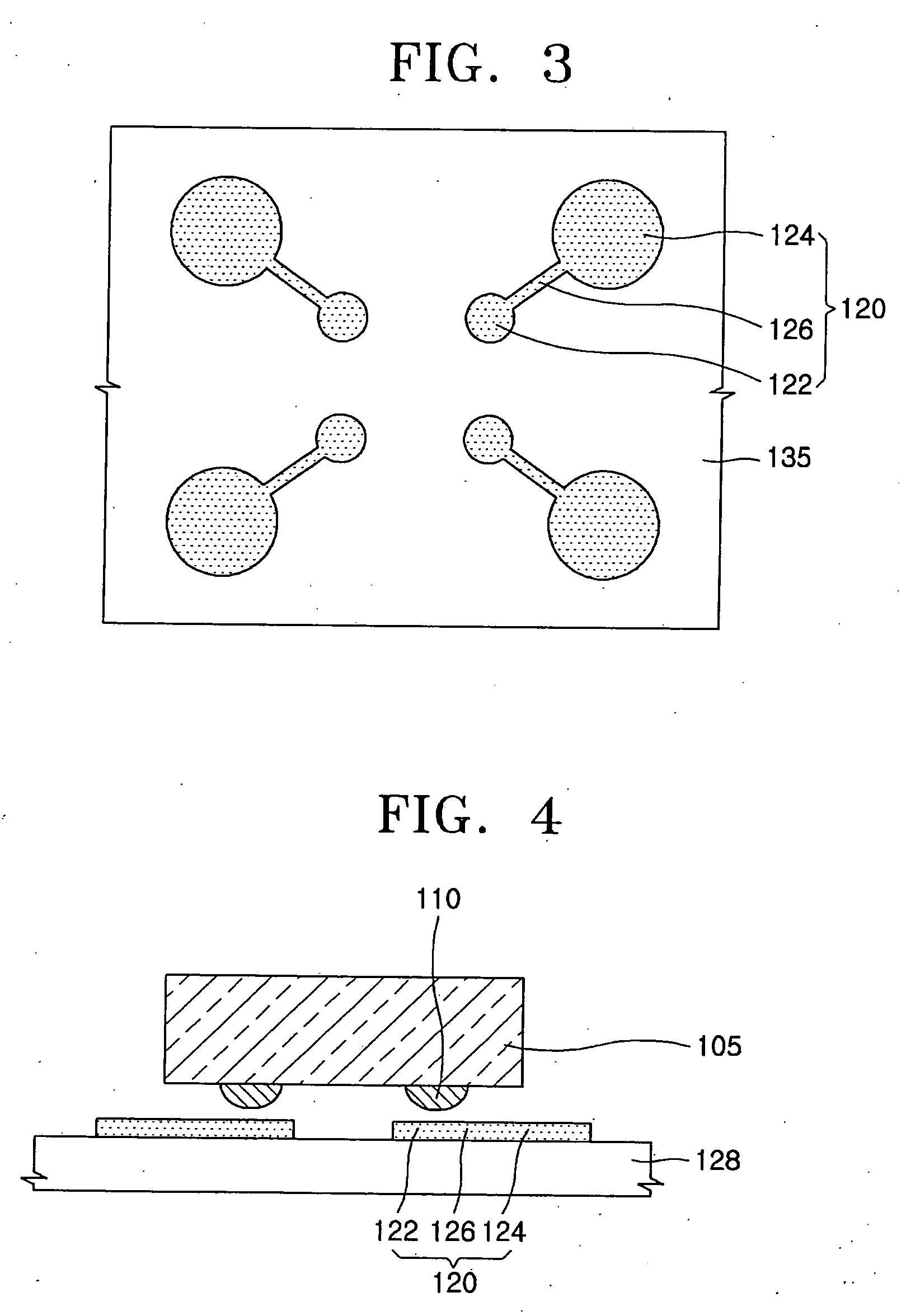
[0025]FIG. 1 is a cross-section of a semiconductor package 100 according to an embodiment of the present invention. FIG. 2 is a bottom view of the semiconductor package 100. FIG. 1 may be a cross-section taken along line I-I□ of FIG. 2.

[0026] Referring to FIG. 1, a plurality of bumps 110 are formed on a bottom surface of a semiconductor chip 105. For example, the bumps 110 may be formed on metal pads (not shown) of the sem...


PUM


Abstract

Provided are a semiconductor package which is small in size but includes a large number of terminals disposed at intervals equal to or greater than a minimum pitch, and a method of fabricating the semiconductor package. The semiconductor package includes a semiconductor chip having a bottom surface on which a plurality of bumps are formed, redistribution layer patterns formed under the semiconductor chip and each including a first part electrically connected to at least one of the bumps and a second part electrically connected to the first part, an encapsulation layer surrounding at least a top surface of the semiconductor chip, and a patterned insulating layer formed below the redistribution layer patterns and exposing at least parts of the second parts of the redistribution layer patterns.

Description

BACKGROUND OF THE INVENTION [0001] 1. Field of the Invention [0002] The present invention relates to a semiconductor device, and more particularly, to a semiconductor package for protecting a semiconductor chip and connecting the semiconductor chip with an external device. [0003] 2. Description of the Related Art [0004] As the integration density of semiconductor chips increases, the number of pads of each semiconductor chip increases. However, semiconductor packages are being continuously demanded to be smaller and lighter with an increasing demand for portable semiconductor products. For example, a chip scale package (CSP) can reduce the size of a semiconductor package by forming terminals on pads of a semiconductor chip. [0005] However, the terminals of the CSP are required to be large enough to form a stable electrical contact with an external device and to be separated from one another by suitable pitches. For example, when the terminals of the CSP are connected to an external ...

Claims


Application Information

Patent Timeline
IPC IPC(8): H01L23/488H01L21/58
CPCH01L21/568H01L21/6835H01L2924/07811H01L2224/16225H01L2924/00013H01L2224/29355H01L2224/29347H01L2224/29344H01L2924/0665H01L2924/014H01L2924/01033H01L2224/2919H01L24/29H01L2924/15173H01L2924/14H01L2924/12044H01L2924/0781H01L2924/01082H01L2924/01079H01L2924/01078H01L2924/01029H01L23/49541H01L24/83H01L2224/16H01L2224/73204H01L2224/838H01L2924/01013H01L2924/00014H01L2924/00H01L2224/29099H01L2224/29199H01L2224/29299H01L2224/2929H01L2924/181H01L23/12
Inventor CHOI, SOUNG-YONGPARK, MIN-HYO
Owner SEMICON COMPONENTS IND LLC
Why Eureka
Try Eureka