Output circuit of a memory and method thereof

a technology of output circuit and memory, which is applied in the direction of information storage, static storage, digital storage, etc., to achieve the effect of improving the performance of the sram and shortening the access time of the sram

Active Publication Date: 2007-05-24
VIA TECH INC
View PDF6 Cites 37 Cited by
  • Summary
  • Abstract
  • Description
  • Claims
  • Application Information

AI Technical Summary

Benefits of technology

[0007] The invention provides an output circuit of a memory which can shorten the access time of a SRAM and improve the performance of the SRAM

Problems solved by technology

Since the driving ability of a SRAM cell is weak, the latency time caused by the parasitic capacitors is a key factor affecting the access time of a SRAM.

Method used


Image

  • Output circuit of a memory and method thereof
  • Output circuit of a memory and method thereof
  • Output circuit of a memory and method thereof

Examples


Embodiment Construction

[0019] The following description is of the best-contemplated mode of carrying out the invention. This description is made for the purpose of illustrating the general principles of the invention and should not be taken in a limiting sense. The scope of the invention is best determined by reference to the appended claims.

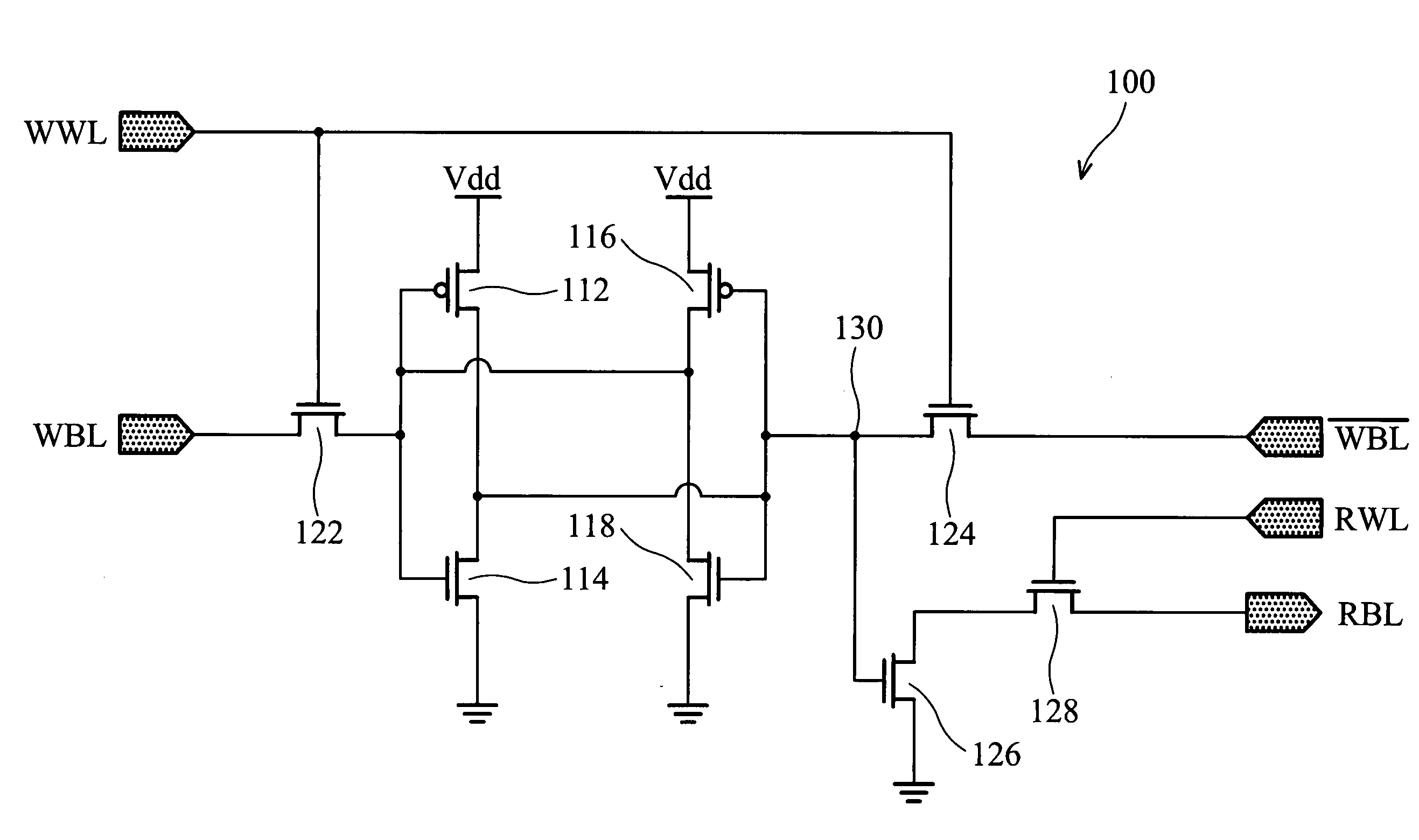
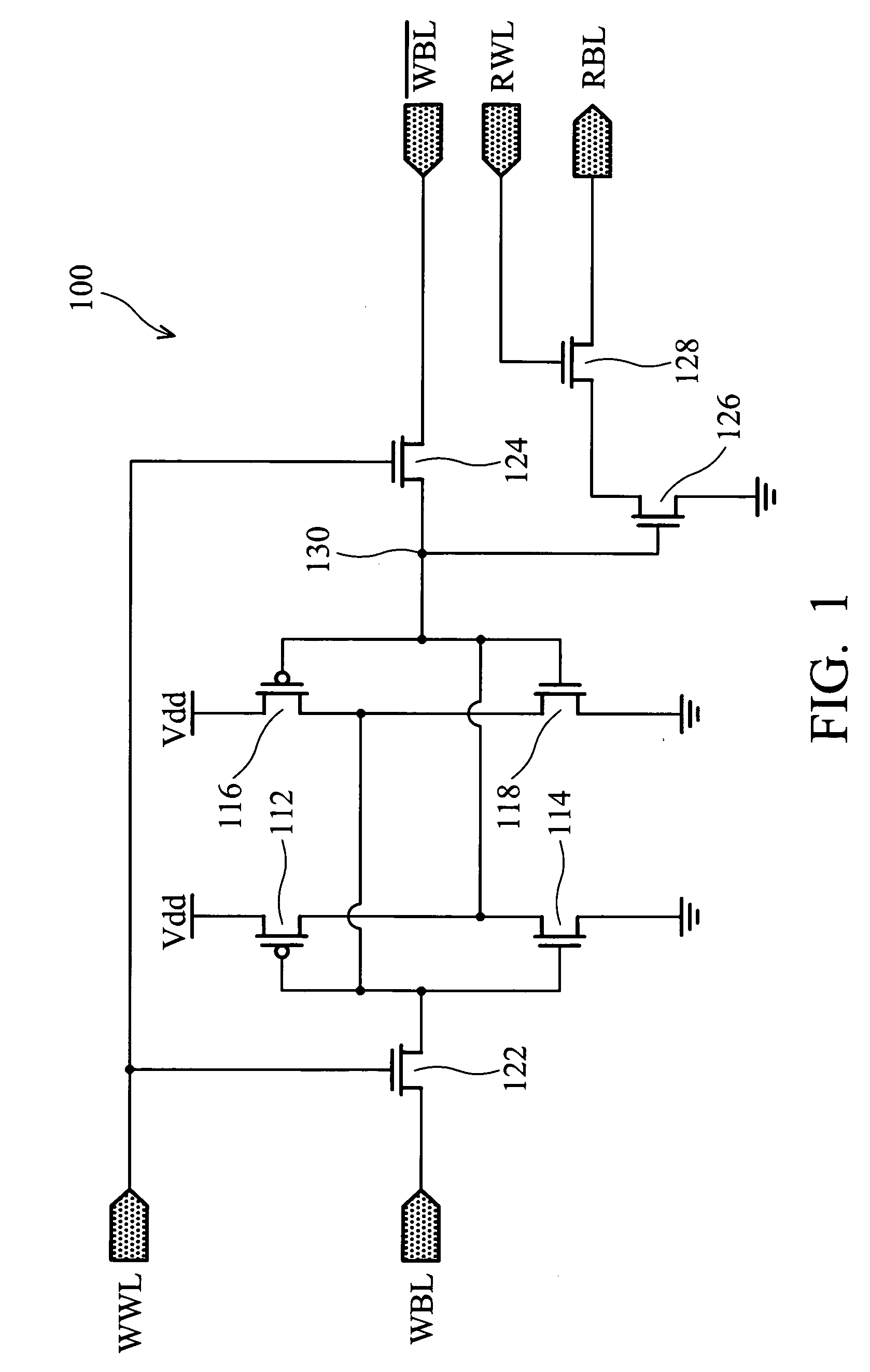
[0020]FIG. 1 is a circuit diagram of a SRAM cell 100. SRAM cell 100 is a dual port cell with eight transistors and a single output terminal. The eight transistors include pull-up transistors 112 and 116, pull-down transistors 114 and 118, pass gate transistors 122 and 124, and read port transistors 126 and 128. The pull-up transistors 112 and 116 are PMOS transistors, the pull-down transistors 114 and 118, the pass gate transistors 122 and 124, and the read port transistors 126 and 128 are NMOS transistors.

[0021] Sources of the pull-up transistors 112 and 116 are respectively coupled to a voltage source Vdd. Drain of the pull-up transistor 112 is coupled with the so...


PUM


Abstract

An output circuit of a memory is provided. The output circuit includes a first pre-charge circuit, coupled to a read bit line which is coupled to a plurality of memory cells, pre-charging the voltage of the read bit line to a logic high level before a stored bit of a target memory cell is read to the read bit line, wherein the target memory cell is one of the plurality of memory cells, and a sense amplifier, coupled to the read bit line, detecting the voltage of the read bit line after the stored bit of the target memory cell is read to the read bit line, and comparing the voltage of the read bit line with the logic high level to respectively generate a comparison result signal and an inverse comparison result signal to a first output node and a second output node.

Description

BACKGROUND OF THE INVENTION [0001] 1. Field of the Invention [0002] The invention relates to an output circuit of a memory and a method thereof; more particularly, the invention relates to an output circuit and method thereof for a static random access memory (SRAM). [0003] 2. Description of the Related Art [0004] Most memory data is stored in the form of binary bits with each bit stored in a memory cell as 0 or 1. The memory cells are arranged in a rectangular matrix and form the principle part of the memory. Before writing data to a specific memory cell, the memory cell is selected by an address latch circuit, and the bit is then written into the memory cell. Before reading data from a specific memory cell, the memory cell is selected by the address latch circuit, and the bit stored in the memory cell is then outputted in the form of current or voltage through the output circuit. Because the current or voltage outputted from the memory cell is very weak, it is amplified by a curre...

Claims


Application Information

Patent Timeline
Patent Type & Authority Applications(United States)
IPC IPC(8): G11C7/00
CPCG11C7/1051G11C7/106G11C7/12G11C11/419
Inventor HUANG, CHAO-SHENG
Owner VIA TECH INC
Why Eureka
Try Eureka