Analytical microchip

a microchip and analytical technology, applied in the field of analytical microchips, can solve the problems of insufficient detection reproducibility and difficulty in injecting an accurate amount of solid particles into the chip, and achieve the effects of enhancing detection accuracy, preventing migration and fluctuation of solid particles, and facilitating production

Inactive Publication Date: 2007-05-24
SHARP KK
View PDF6 Cites 7 Cited by
  • Summary
  • Abstract
  • Description
  • Claims
  • Application Information

AI Technical Summary

Benefits of technology

[0030] These advantageous effects are more reliably secured in the third aspect, where the first damming portion and the second damming portion are provided. This is because the first damming portion and the second damming portion reliably prevent migration and fluctuation of solid particles. If the first damming portion and the second damming portion are not provided in the chip, a means of preventing runoff of solid particles is preferably provided outside the chip.
[0031] According to the second aspect, where the test-solution introducing path and the test-solution discharging path extend in opposite directions from the reaction path, the flow of the test solution is not localized either on the side of the test-solution introducing path or the side of the test-solution discharging path. This enhances detection accuracy. Further, this structure is easily produced by superposing two substrates, the main substrate and back substrate.
[0032] As a reactant used in the analytical microchip according to the present invention, one of guest / hose molecules is used as a chemical material, and as a biological material, one of substances with binding specificity such as antigen-antibody-reaction materials is used. While as an antigen-antibody-reaction material a protein such as antigen-antibody, a protein such as a fragment of the foregoing protein, or the like can be used, other materials than a protein can be made a target such as a fine chemical material including environmental hormones.
[0033] The terms “an upper stream side” and “a lower stream side”, used above, are concepts based on the flow of the test solution introduced into the reaction path from outside of the chip for reaction in the chip, and are used in the same manner throughout the specification.
[0034] The above analytical microchip according to the present invention may further have: a washing aperture for injecting a washing solution to wash a group of solid particles in the reaction path out of the chip through the particle injection aperture, the washing aperture being provided at the lower stream end of the reaction path; and a third damming portion for damming solid particles, the third damming portion being provided on the upper stream side relative to the washing aperture and on the side of the washing aperture relative to the test-solution discharging path (fourth aspect).
[0035] In this aspect, a damming portion is provided on the lowermost stream side of the reaction path, and thus the desired particle-filled area can be formed using a smaller amount of solid particles. Also, the damming portion prevents the filled structure from crumbling through the flow of the test solution, thereby further enhancing detection stability. If the third damming portion is not provided in the chip, a means of preventing runoff of solid particles is preferably provided outside the chip. One example of such a means is placing a net over the washing aperture.

Problems solved by technology

As described above, while analytical microchips using solid particles such as beads are advantageous because they have simple structures, are easy to handle, and provide highly sensitive detection in a short time, it is difficult to inject an accurate amount of solid particles into the chip.
This poses the problem of insufficient detection reproducibility.

Method used


Image

  • Analytical microchip
  • Analytical microchip
  • Analytical microchip

Examples


embodiment 1

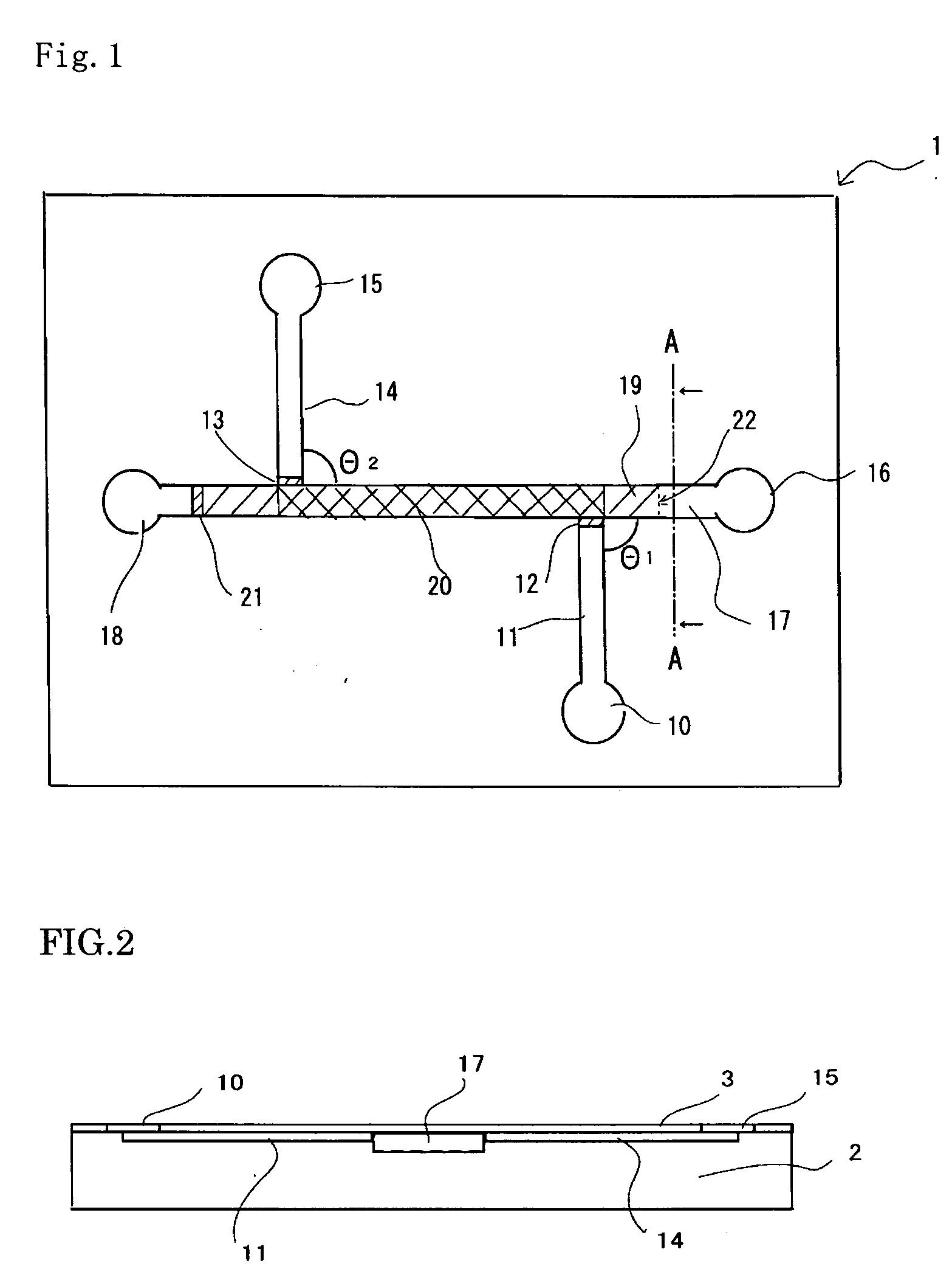
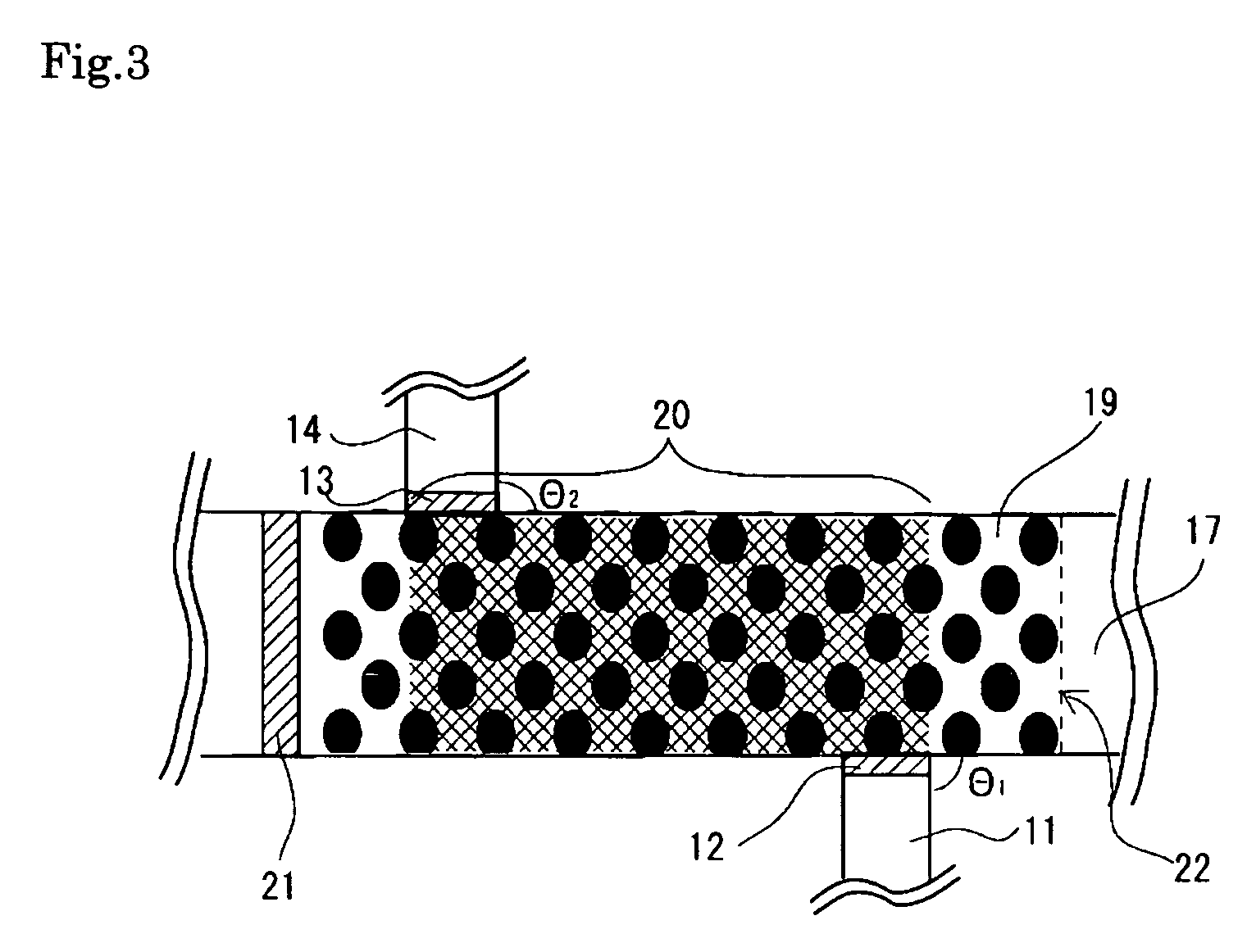
[0087] An analytical microchip 1 according to embodiment 1 will be described with reference to FIGS. 1 to 3. FIG. 1 is a plan view of the analytical microchip 1, FIG. 2 is a sectional view of the analytical microchip 1 taken along the line A-A, and FIG. 3 is a partially enlarged view mainly of a solid-particle-filled area of the analytical microchip 1.

[0088]

[0089] First, the main portions (the essential constituent elements of the present invention) of the analytical microchip 1 will be described referring to FIG. 3. The analytical microchip 1 according to the present invention has: a reaction path 17 composed of a depression groove formed on a main substrate 2; a particle-filled area 19 formed by filling the reaction path 17 with a group of solid particles having reactants immobilized on the surfaces of the solid particles; a test-solution introducing path 11 for introducing a test solution into the reaction path 17 from outside of the microchip; a test-solution discharging path 1...

embodiment 2

[0126] Embodiment 2 will be described with reference to FIG. 4, which is a plan view of a microchip according to embodiment 2, showing the main portions of the microchip. In embodiment 2, the structures of the reaction path, the test-solution introducing path, and the test-solution discharging path shown in FIG. 1 are respectively replaced with the structures shown in FIG. 4. The rest are as described in embodiment 1.

[0127] As shown in FIG. 4, in the structure of a microchip according to embodiment 2, a test-solution introducing paths 51 has a multi-stepwise furcation structure furcating into branches in a multi-stepwise manner (a three-stepwise furcation in FIG. 4) toward the lower stream. The test-solution introducing path 51, which has a multi-stepwise furcation structure, is located so as to be orthogonal to a reaction path 60. At one end (the right side in FIG. 4) of the reaction path 60, a first washing aperture is provided, and at the other end of the reaction path 60, a sec...

embodiment 3

[0132] In embodiment 3, the test-solution discharging path having the inverted-triangle tapering structure in embodiment 2 is replaced with a discharging path having an inverse multi-stepwise furcation structure as shown in FIG. 5. The rest are as described in embodiment 1 or 2. Specifically, in embodiment 3, the test-solution discharging path 85 has an inverse multi-stepwise furcation structure furcating into a plurality of branches in an equal to or more than two steps (three steps in FIG. 5) from the lowermost stream side toward a reaction path 88. A group of second damming portions 84 are provided in the lowermost-stream portions (points of connection with the reaction path 88) of the discharging path having an inverse multi-stepwise furcation structure.

[0133] The uppermost-stream-side flow paths of the test-solution discharging path 85 having an inverse multi-stepwise furcation structure are arranged to oppose to the lowermost-stream-side flow paths of a test-solution introduc...


PUM

PropertyMeasurementUnit
thicknessaaaaaaaaaa
diameteraaaaaaaaaa
groove depthaaaaaaaaaa

Abstract

The detection accuracy and detection reproducibility of an analytical microchip utilizing beads are improved. To this end the analytical microchip has a reaction path 17 having a particle-filled area 19 filled with a group of solid particles, a test-solution introducing path 11 for introducing a test solution into the reaction path, a test-solution discharging path 14 for discharging a test solution inside the reaction path to outside of the microchip, and a particle injection aperture 16 provided on one end side of the reaction path 17. The test-solution discharging path 14 has a direct communication with the particle-filled area 19 in the reaction path 17. The test-solution introducing path 11 has a direct communication with the reaction path 17 on the upper stream side relative to the test-solution discharging path 14 and within the upper-stream-side end surface 22 of the particle-filled area 19. A first damming portion 12 is provided at the point of connection of the test-solution introducing path 11 and the reaction path 17. A second damming portion 13 is provided at the point of connection of the test-solution discharging path 14 and the reaction path 17.

Description

BACKGROUND OF THE INVENTION [0001] 1) Field of the Invention [0002] The present invention relates to analytical microchips used for micro-chemical analysis and microreactors. [0003] 2) Description of the Related Art [0004] In recent years, micromachining technology (Micro Electro-Mechanical System, MEMS), which utilizes microprocessing technology of semiconductors, is drawing attention. In the field of analytical chemistry, micromachining technology (Micro Total Analytical System, μ-TAS) is rapidly developing for protein and genes in biochemistry. In the latter technology, which uses antigen-antibody reactions, a reactant (e.g., an antibody) is immobilized directly on a reaction portion, and a solution containing an antigen is allowed to flow in this portion, thereby obtaining a antigen-antibody reaction. However, with this conventional method, the reaction surface area cannot be sufficiently enlarged, making it impossible to reliably bring the solution containing the antigen into c...

Claims


Application Information

Patent Timeline
Patent Type & Authority Applications(United States)
IPC IPC(8): G01N31/22
CPCB01L3/502715B01L3/502753B01L3/502761B01L2200/0668B01L2300/0816B01L2300/0877B01L2400/0487
Inventor SHIMIZU, YUICHIROHASHIGUCHI, KAZUO
Owner SHARP KK
Why Eureka
Try Eureka