Display device

a display device and display technology, applied in static indicating devices, instruments, electroluminescent light sources, etc., can solve the problems of reducing yield, increasing the number of defects, and increasing the complexity of the wire structure, so as to reduce the number of wires, improve the aperture ratio, and simplify the manufacturing process

Inactive Publication Date: 2007-05-31
SEMICON ENERGY LAB CO LTD
View PDF13 Cites 75 Cited by
  • Summary
  • Abstract
  • Description
  • Claims
  • Application Information

AI Technical Summary

Benefits of technology

[0006] In the above-described pixel configuration, however, the aperture ratio of each pixel may be reduced since it is necessary to form a plurality of wires within each pixel. Further, the wires are densely-disposed, thereby the wire structure becomes complex and dense. Therefore, when the process becomes difficult and complex, the number of defects might be increased, and a yield is decreased.
[0007] In view of the foregoing, it is an object of the present invention to provide a high-performance and highly reliable display device with a high aperture ratio, including light-emitting elements, and a manufacturing method thereof. In addition, it is another object of the present invention to provide a technique for manufacturing a display device at a low cost with high productivity.
[0014] By using the present invention, since the number of wires can be reduced in each pixel, the aperture ratio can be improved and the manufacturing process can be simplified. Consequently, such a highly reliable display device can be manufactured with a high yield. In addition, the present invention can manufacture a display device at a low cost with good productivity.

Problems solved by technology

Further, the wires are densely-disposed, thereby the wire structure becomes complex and dense.
Therefore, when the process becomes difficult and complex, the number of defects might be increased, and a yield is decreased.

Method used


Image

  • Display device
  • Display device
  • Display device

Examples


embodiment mode 1

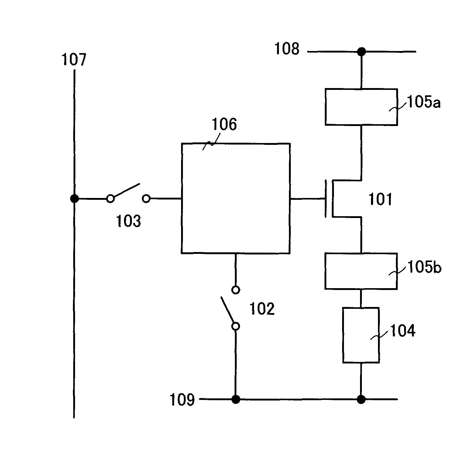
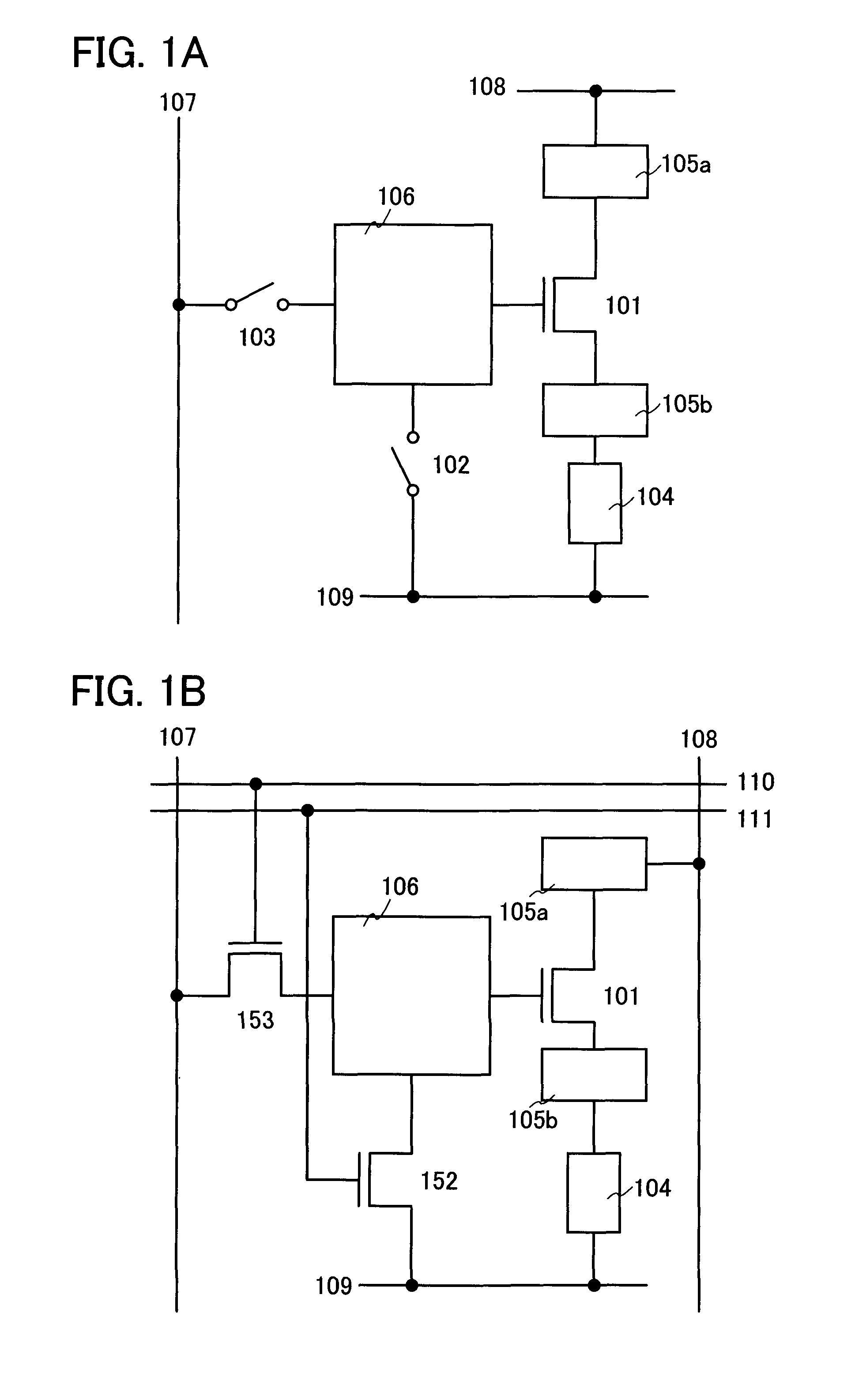
[0048] An embodiment mode of the present invention will be described using FIGS. 1A and 1B. A pixel shown in FIG. 1A includes a transistor 101, switches 102 and 103, a light-emitting element 104, controlling circuits 105a and 105b, and a compensating circuit 106. The present invention is not limited to the configuration of FIGS. 1A and 1B; all of the above-described components are not necessarily included.

[0049]FIG. 1B shows an example in which transistors 152 and 153 are used as the switches 102 and 103 respectively in FIG. 1A. The transistor 101 is a transistor for controlling light-emission of the light-emitting element, the transistor 153 is a transistor for controlling a video signal input to the pixel, a wire 107 is a wire for sending the video signal, a wire 108 is a wire maintained at a certain potential, and a wire 109 is a wire maintained at a certain potential. Respective potentials of the wires 108 and 109 are different, and have a potential difference.

[0050] Each cond...

embodiment mode 2

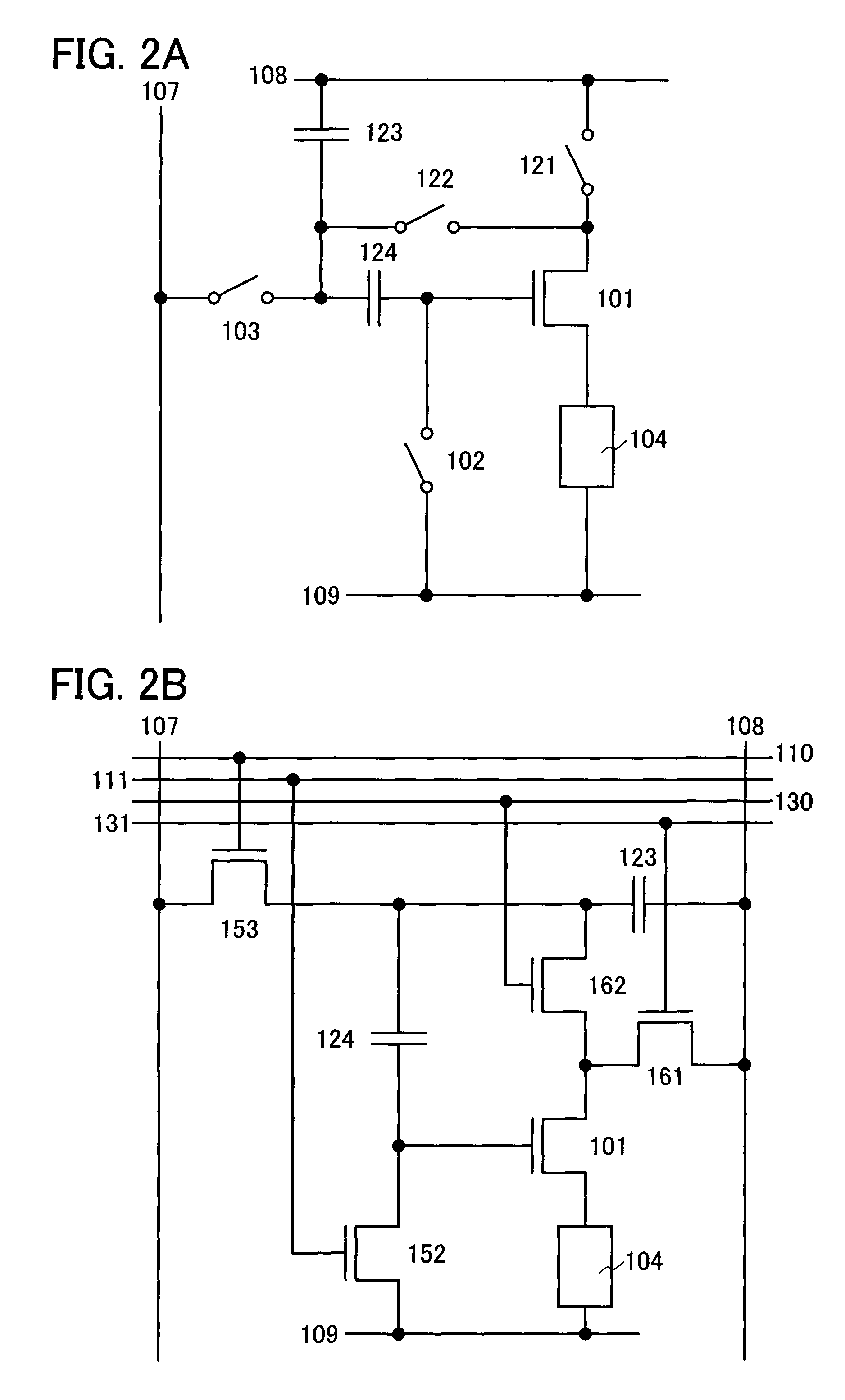
[0096] A pixel configuration which is different from the above embodiment mode will be described using FIG. 4A.

[0097] A pixel includes transistors 8010 to 8015, capacitors 8016 and 8017, and a light-emitting element 8000. According to this pixel, one of a source and a drain of the transistor 8010 and one of a first electrode and a second electrode of the light-emitting element 8000 are connected to the same wire 8009.

[0098] In the pixel shown in FIG. 4A, the transistor 8012 and the capacitors 8016 and 8017 correspond to the compensating circuit 106 in FIG. 1B, and the transistors 8013 and 8015 correspond to the controlling circuit 105a in FIG. 1B.

[0099] ON / OFF of the transistors 8010 to 8013 and 8015 are controlled by signals inputted though wires 8003 to 8006. Light emission / non-light emission of the light-emitting element 8000 is controlled by a video signal inputted though a wire 8001. Further, a power source is supplied from a wire 8002 maintained at a certain potential to th...

embodiment mode 3

[0100] A pixel configuration which is different from the above embodiment mode will be described using FIG. 4B.

[0101] A pixel includes transistors 8110 to 8115, a capacitor 8116, and a light-emitting element 8100. The pixel may further include a capacitor 8117. According to this pixel, one of a source and a drain of the transistor 8110 and one of a first electrode and a second electrode of the light-emitting element 8100 are connected to the same wire 8109.

[0102] In the pixel shown in FIG. 4B, the transistors 8112 and 8113 and the capacitors 8116 and 8117 correspond to the compensating circuit 106 in FIG. 1B, and the transistor 8115 corresponds to the controlling circuit 105b in FIG. 1B.

[0103] ON / OFF of the transistors 8110 to 8113 and 8115 are controlled by signals inputted though wires 8103 to 8106. Light emission / non-light emission of the light-emitting element 8100 is controlled by a video signal inputted though a wire 8101. Further, a power source is supplied from a wire 810...


PUM


Abstract

To provide a high-performance and highly reliable display device with a high aperture ratio, including light-emitting elements, and a manufacturing method thereof, and a technique for manufacturing such a display device at a low cost with high productivity. A compensating circuit, a light-emitting element, a switch, and a transistor are included, in which one terminal of the switch is electrically connected to the compensating circuit, a gate of the transistor is electrically connected to the compensating circuit, one of a source and a drain of the transistor is electrically connected to a first electrode of the light-emitting element, the other of the source and the drain of the transistor is maintained at a certain potential, and a second electrode of the light-emitting element and the other terminal of the switch are electrically connected to the same wire.

Description

BACKGROUND OF THE PRESENT INVENTION [0001] 1. Field of the Present Invention [0002] The present invention relates to a display device using a light-emitting element. [0003] 2. Description of the Related Art [0004] In recent years, development of an electroluminescence (Electro Luminescence) display device in which thin film transistors (hereafter also referred to as “TFTs”) are integrated over a substrate has progressed. In such a display device, thin film transistors are manufactured over a substrate by using thin-film formation technology and a light-emitting element (electroluminescence (hereinafter also referred to as “EL”) element) is formed as a display element over various circuits including the thin film transistors. [0005] In pixels of a display device using light-emitting elements, respective amounts of current flowing into the light-emitting elements vary depending on variations of electrical characteristics such as each threshold voltage of TFTs for forming the pixels, s...

Claims


Application Information

Patent Timeline
Patent Type & Authority Applications(United States)
IPC IPC(8): G09G3/32
CPCG09G3/3233G09G3/325G09G2300/0465G09G2300/0819G09G2300/0842G09G2300/0852G09G2300/0861G09G2310/0251G09G2320/043G09G2330/04H01L27/3244H10K59/12G09G3/30G09G3/32H05B33/26G09G3/20
Inventor KIMURA, HAJIME
Owner SEMICON ENERGY LAB CO LTD
Why Eureka
Try Eureka