Imaging Device

a technology of imaging device and pixel sensitivity, which is applied in the direction of color signal processing circuit, television system scanning details, television system, etc., can solve the problems of increasing the manufacturing cost of imaging device, unlikely to be able to normally operate, and flicker, so as to reduce flicker, reduce the occurrence of flicker, and change the pixel sensitivity

Inactive Publication Date: 2007-05-31
FUNAI ELECTRIC CO LTD
View PDF8 Cites 14 Cited by
  • Summary
  • Abstract
  • Description
  • Claims
  • Application Information

AI Technical Summary

Benefits of technology

[0012] It is an object of the present invention to provide an imaging device with reduced occurrence of flicker that...

Problems solved by technology

On the other hand, in high brightness mode where an image received by the imaging device is in a high brightness range, flicker is likely to occur.
In this high brightness mode, the imaging device is unlikely to be able to normally operate if the photodiode has a normal o...

Method used


Image

  • Imaging Device
  • Imaging Device
  • Imaging Device

Examples


first embodiment

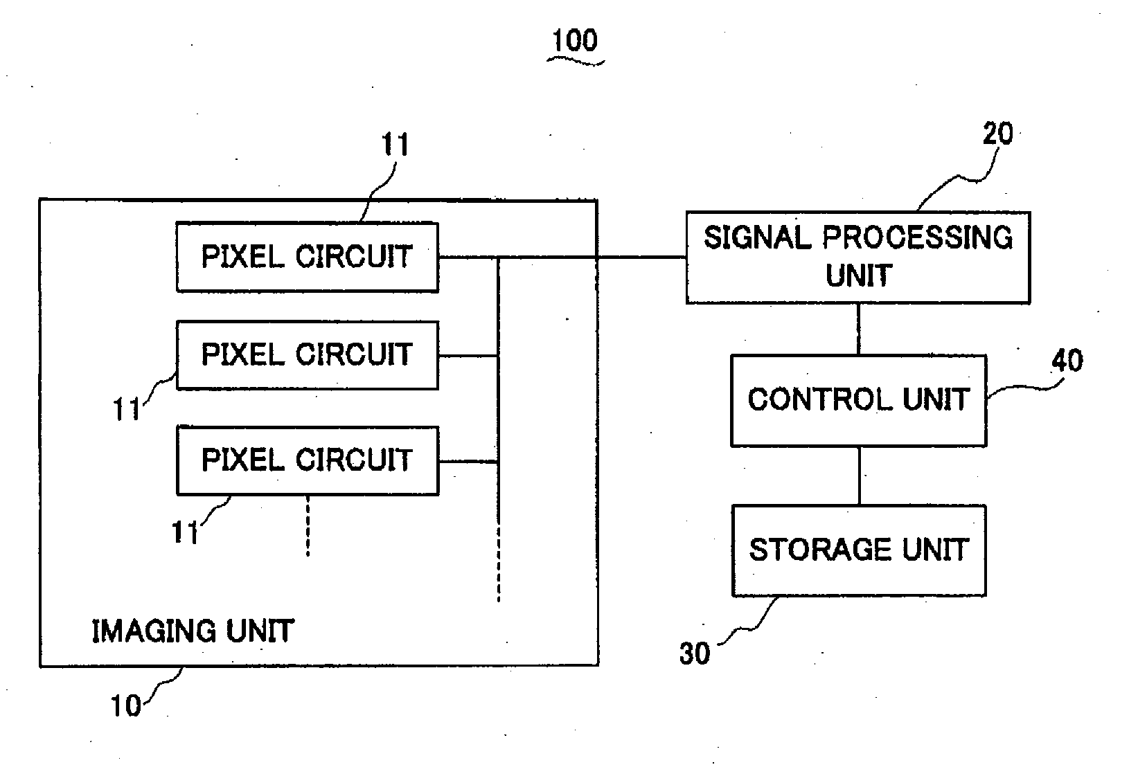
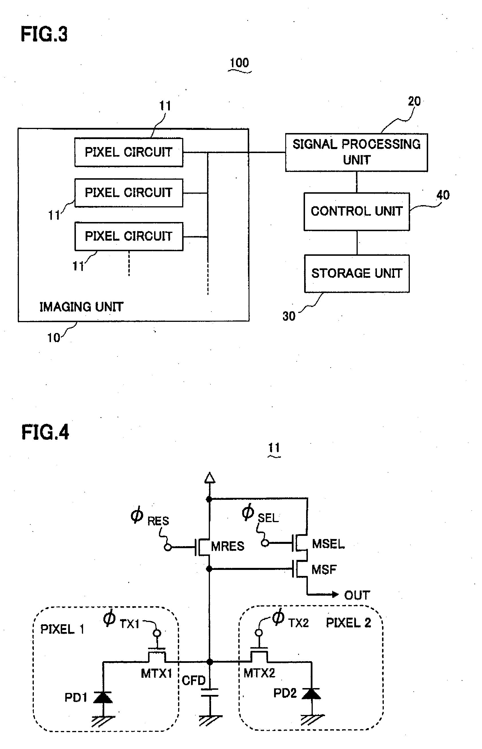
[0043] An imaging device according to a First Embodiment of the present invention will be described with reference to FIG. 3 to FIG. 9. FIG. 3 is a schematic block diagram of an imaging device 100 according to the First Embodiment of the present invention. The imaging device 100 comprises: an imaging unit 10 having multiple pixels for imaging an image and outputting an electrical signal corresponding to the image; a signal processing unit 20 for processing the electrical signal output from the imaging unit 10; a storage unit 30 for storing electrical signals output from the signal processing unit 20; a control unit 40 for controlling respective units and elements of the imaging device 100; and so on. The imaging unit 10 has many pixel circuits 11.

[0044] In a general pixel circuit, various components are provided for each pixel, in which the various components include photodiodes, transfer switches, capacitances, amplifying transistors, reset switches and selection switches as will ...

second embodiment

[0062] Next, a Second Embodiment of the present invention will be described with reference to FIG. 10 to FIG. 18. FIG. 10 is a schematic circuit diagram of an example of a pixel circuit 11 applicable to an imaging device 100 of the Second Embodiment which is similar to the imaging device 100 of the First Embodiment except for the points as will be described below. Pixels 1, 2, 3, 4 (one of multiple units each of four pixels) respectively have photodiodes photoelectric conversion units) PD1, PD2, PD3, PD4 for converting light to electrical signals as well as transfer switches (transfer means) MTX1, MTX2, MTX3, MTX4 for transferring signal charges output from the photodiodes PD1, PD2, PD3, PD4.

[0063] In the pixel circuit 11 of FIG. 10, the four adjacent pixels, pixels 1 to 4, among many pixels (multiple units of four pixels) use various components in common other than the photodiodes PD1, PD2, PD3, PD4 and transfer switches MTX1, MTX2, MTX3, MTX4, so as to reduce the size of each pix...

third embodiment

[0080] Next, a Third Embodiment of the present invention will be described with reference to FIG. 19 and FIG. 20. The Third Embodiment is the same as the Second Embodiment in the structure of a pixel circuit 11 in an imaging device 100, but is different from the Second Embodiment in a method of driving the pixel circuit 11, particularly in the operation of the pixel circuit 11 in high brightness mode. All-pixel read mode and normal brightness mode in the pixel downsampling read mode in the Third Embodiment are performed in the same manner as in the Second Embodiment. That is, the pixel circuit 11 in the Third Embodiment operates based on the timing charts shown in FIG. 11 and FIG. 12 in the all-pixel read mode and in the normal brightness mode in the pixel downsampling read mode, respectively.

[0081]FIG. 19 is a timing chart showing an operation of the pixel circuit 11 of FIG. 10 in high brightness mode in pixel downsampling read mode, in which the pixel 1 and the pixel 2 are used a...


PUM


Abstract

In an imaging device having an all-pixel read mode for reading signals from all pixels and a pixel downsampling read mode for reading signals by appropriately discarding pixels, adjacent ones of pixels use a floating diffusion capacitance, an amplifying transistor, a reset switch and a selection switch in common. In the pixel downsampling read mode, not only a primary capacitance but also a photodiode in each pixel to be discarded are used as capacitances for storing signal charges transferred from transfer switches. This makes it possible to lower the gate voltage of the amplifying transistor as compared with the case of using only the primary capacitance as a capacitance for storing signal charges transferred from a transfer switch to reduce the sensitivity of the pixels, thereby reducing the occurrence of flicker.

Description

BACKGROUND OF THE INVENTION [0001] 1. Field of the Invention [0002] The present invention relates to an imaging device with reduced occurrence of flicker. [0003] 2. Description of the Related Art [0004] Various studies have been made for an imaging device, particularly for a method of reading signals therein. For example, Japanese Laid-open Patent Publication 2000-165754 discloses a signal reading method for the purpose of increasing dynamic range. FIG. 1 and FIG. 2 correspond to FIG. 12 and FIG. 13 of the Patent Publication, respectively, which are a diagram of a pixel circuit of the fourth example described therein, and a timing chart showing the operation of the pixel circuit. The purpose of this signal reading method is not to reduce the occurrence of flicker, but to increase dynamic range as described above. However, since this method can be applied to reduce the occurrence of flicker under the illumination of a fluorescent lamp, this method will be described below as an exampl...

Claims


Application Information

Patent Timeline
IPC IPC(8): H04N5/225H04N9/04H04N5/335H04N5/341H04N5/345H04N5/347H04N5/351H04N5/353H04N5/357H04N5/374H04N5/3745H04N9/07
CPCH04N3/155H04N5/23245H04N5/235H04N5/2357H04N23/667H04N23/745H04N23/70H04N25/445H04N25/59H04N25/778
Inventor OITA, MASAYATANAKA, HIROMICHIKIMATA, MASAFUMI
Owner FUNAI ELECTRIC CO LTD
Why Eureka
Try Eureka