Particle-in-binder X-ray sensitive coating using polyimide binder

a technology of x-ray sensitive coating and particle-in-binder, which is applied in the direction of instruments, non-metal conductors, conductors, etc., can solve the problems of high reactiveness of sub-particle-in-binder materials, high starting power, and chemical instability of sub-particles

Active Publication Date: 2007-05-31
GENERAL ELECTRIC CO
View PDF9 Cites 19 Cited by
  • Summary
  • Abstract
  • Description
  • Claims
  • Application Information

AI Technical Summary

Problems solved by technology

Amorphous selenium (a-Se) has relatively low stopping power for X-rays having energy levels approximately above 30 kVp, and in addition incurs incremental costs due to vacuum vapor deposition of Se.
HgI2 particle-in-binder (PIB) materials tend to be hi...

Method used


Image

  • Particle-in-binder X-ray sensitive coating using polyimide binder
  • Particle-in-binder X-ray sensitive coating using polyimide binder
  • Particle-in-binder X-ray sensitive coating using polyimide binder

Examples


Embodiment Construction

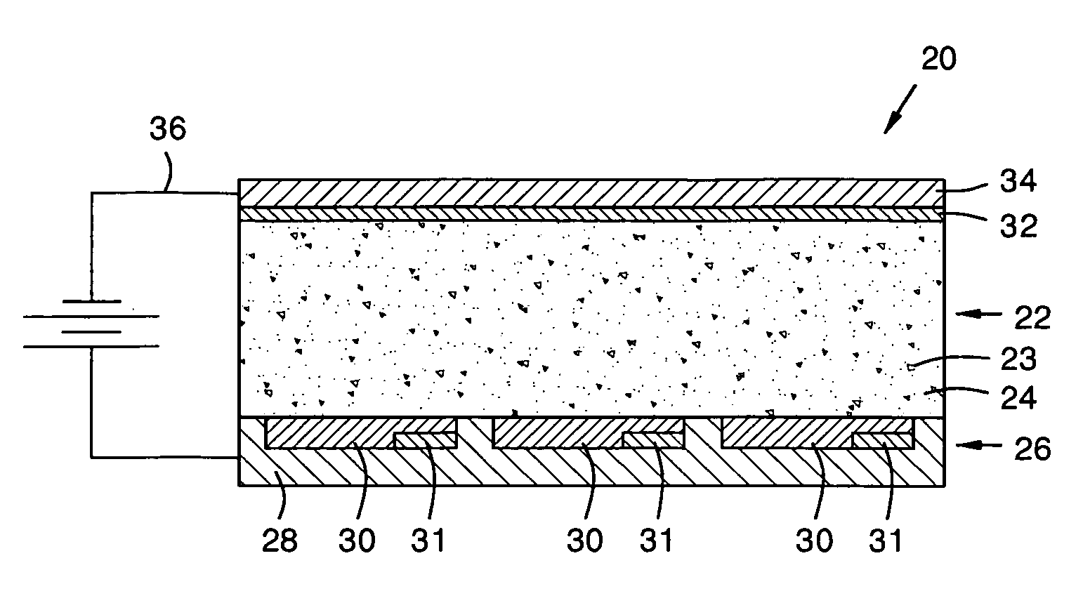
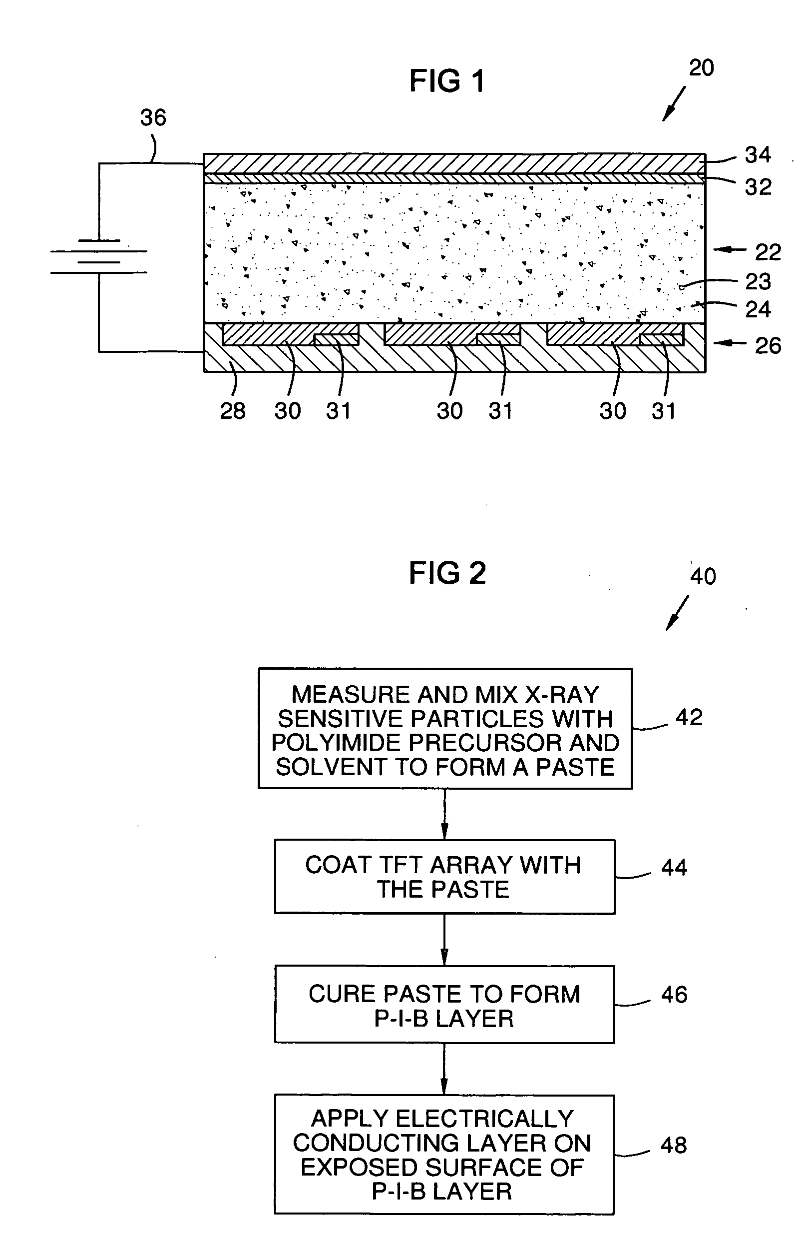
[0008]FIG. 1 illustrates an exemplary flat panel direct conversion X-ray detector according to aspects of the present invention. A thin film transistor (TFT) array 26 comprises a plurality of pixel elements 30 in a substrate 28. Each pixel element 30 may comprise a collector plate, a transistor, and a storage capacitor 31, and may be electrically coupled to a gate line and a data line. The data line may be coupled to an A / D converter to supply digitized data to a computer or processor for image data input, analysis, storage, and display, each of which is well-understood in the art. For readers desirous of general background information, reference is made to a paper titled “Direct-Conversion Flat-Panel X-Ray Image Sensors For Digital Radiography” by S. O. Kasap and J. A. Rowlands, published in Proceedings of the IEEE, Vol. 90, No. 4, April 2002, which paper is herein incorporated by reference in its entirety.

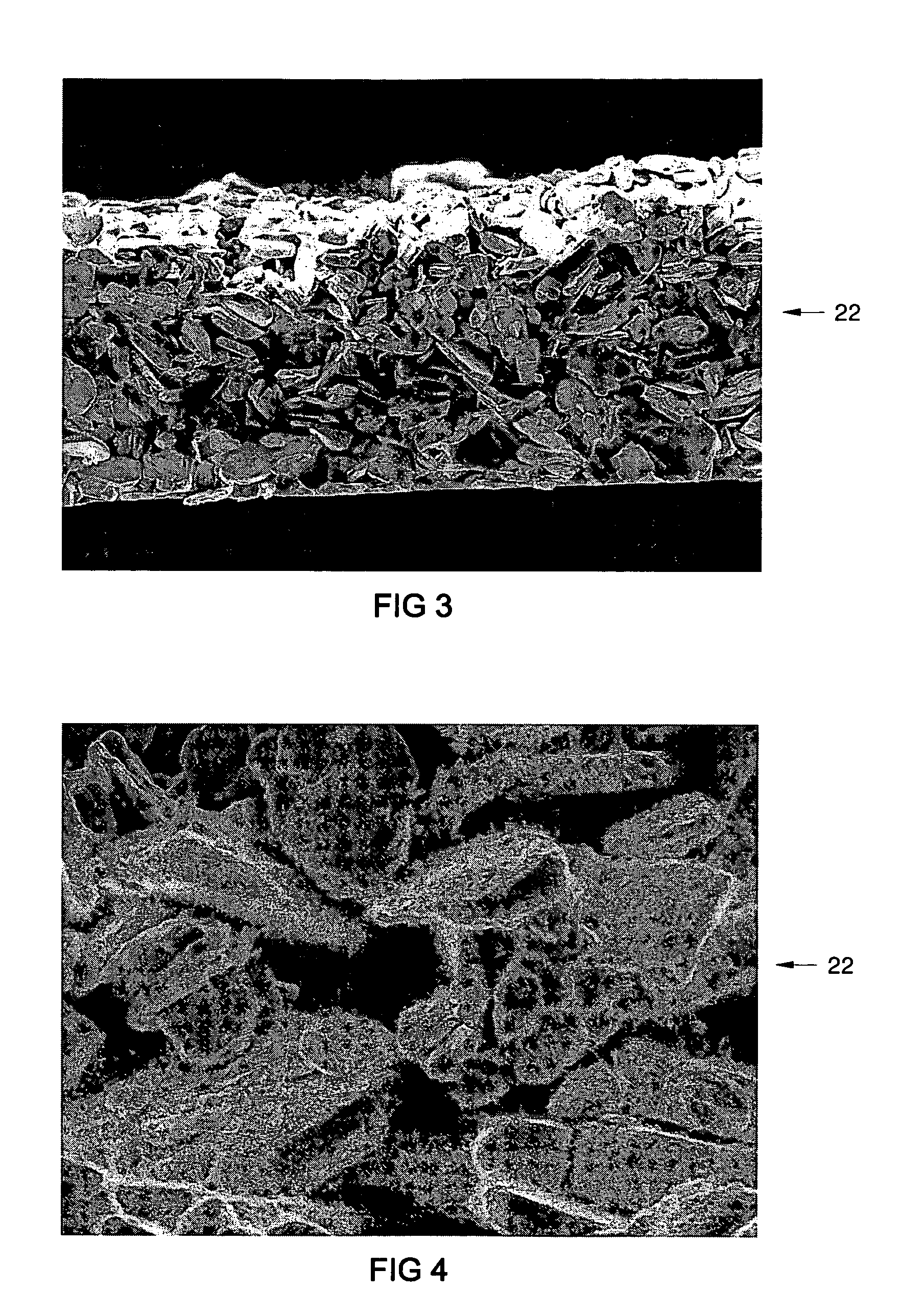
[0009] An X-ray sensitive layer 22 is formed as a coating on the TFT arra...


PUM

PropertyMeasurementUnit
Lengthaaaaaaaaaa
Fractionaaaaaaaaaa
Fractionaaaaaaaaaa

Abstract

An X-ray sensitive coating (22) for a flat panel direct conversion X-ray detector for medical or industrial imaging. A composite particle-in-binder (PIB) material (22) may contain X-ray photoconductive particles (23) such as PbO (lead monoxide) in a binder of polyimide (23). This PIB material may be prepared in precursor paste form, and applied as a coating (22) onto a thin film transistor array (26) having a storage capacitor (31) at each pixel (30). The coating (22) is cured, and an electrically conducting layer (34) is applied to the exposed surface of the coating (22), to provide a bias voltage. X-ray photons striking the photoconductive particles (23) cause localized electrical conduction proportional to the number of photons. This charges respective capacitors (31) that provide image data input to a computer.

Description

FIELD OF THE INVENTION [0001] This invention is generally in the field of direct conversion X-ray imaging, and, more particularly, X-ray sensitive coatings, such as may be used in flat panel direct conversion X-ray detectors for medical and industrial imaging. BACKGROUND OF THE INVENTION [0002] X-ray sensitive coatings for direct conversion X-ray imaging have been made of various photoconductor materials that normally behave as insulators, but upon impingement of X-ray photons directly form an electrical charge without use of intermediary converting materials. A thin film transistor (TFT) array provides electrical charge signals from each of a plurality of pixels to a computer. Prior photoconductor materials and binders used in detectors for direct conversion X-ray imaging have suffered from various disadvantages. Amorphous selenium (a-Se) has relatively low stopping power for X-rays having energy levels approximately above 30 kVp, and in addition incurs incremental costs due to vac...

Claims


Application Information

Patent Timeline
IPC IPC(8): B05D5/12H01B1/12
CPCG01T1/24
Inventor YANOFF, BRIAN DAVIDWU, ZHAOPINGTAO, KUNSUN, YUNFENGXIAO, JUNZHENG, LIPINGPENG, WENQINGLI, JING
Owner GENERAL ELECTRIC CO
Why Eureka
Try Eureka