High-power LED chip packaging structure and fabrication method thereof

a technology of led chips and packaging structures, applied in the field of high-power led chip packaging structures, can solve the problems of inability to dissipate heat produced by, inability to meet the requirements of high-power led chip manufacturing, etc., to achieve superior heat dissipation efficiency and reduce production costs.

Inactive Publication Date: 2007-06-07
HIGH POWER LIGHTING CORP
View PDF12 Cites 78 Cited by
  • Summary
  • Abstract
  • Description
  • Claims
  • Application Information

AI Technical Summary

Benefits of technology

[0008] Accordingly, the major objective of the present invention is to provide a packaging structure and a related fabrication method for packaging a high-power LED chip which, in one way, achieve superior heat dissipation efficiency and, in another way, are applicable in mass production for a significantly reduced production cost.

Problems solved by technology

However, in this conventional structure, the heat produced by the LED chip 16 could only be dissipated through the thin copper foil 15 as resin is not an acceptable thermal conductor.
However, the production process as described above is rather complex and a higher production cost is therefore inevitable.
In addition, the lead frame 12 and the protection lens 20 have to be prepared in advance by molding, leading to a very inflexible production process, let alone the cost involved for the molds.

Method used


Image

  • High-power LED chip packaging structure and fabrication method thereof
  • High-power LED chip packaging structure and fabrication method thereof
  • High-power LED chip packaging structure and fabrication method thereof

Examples


first embodiment

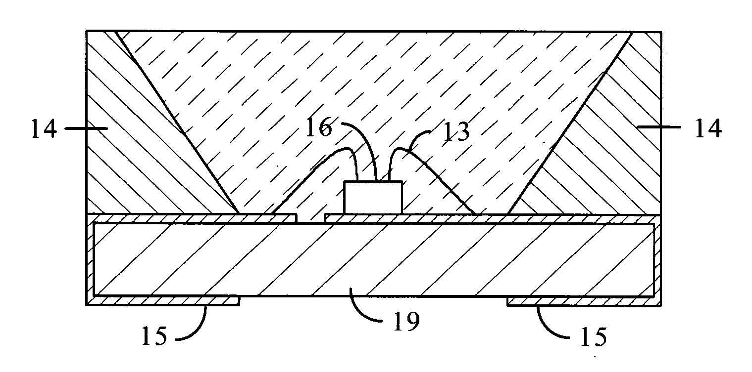
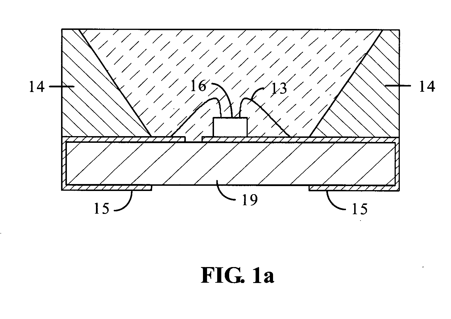
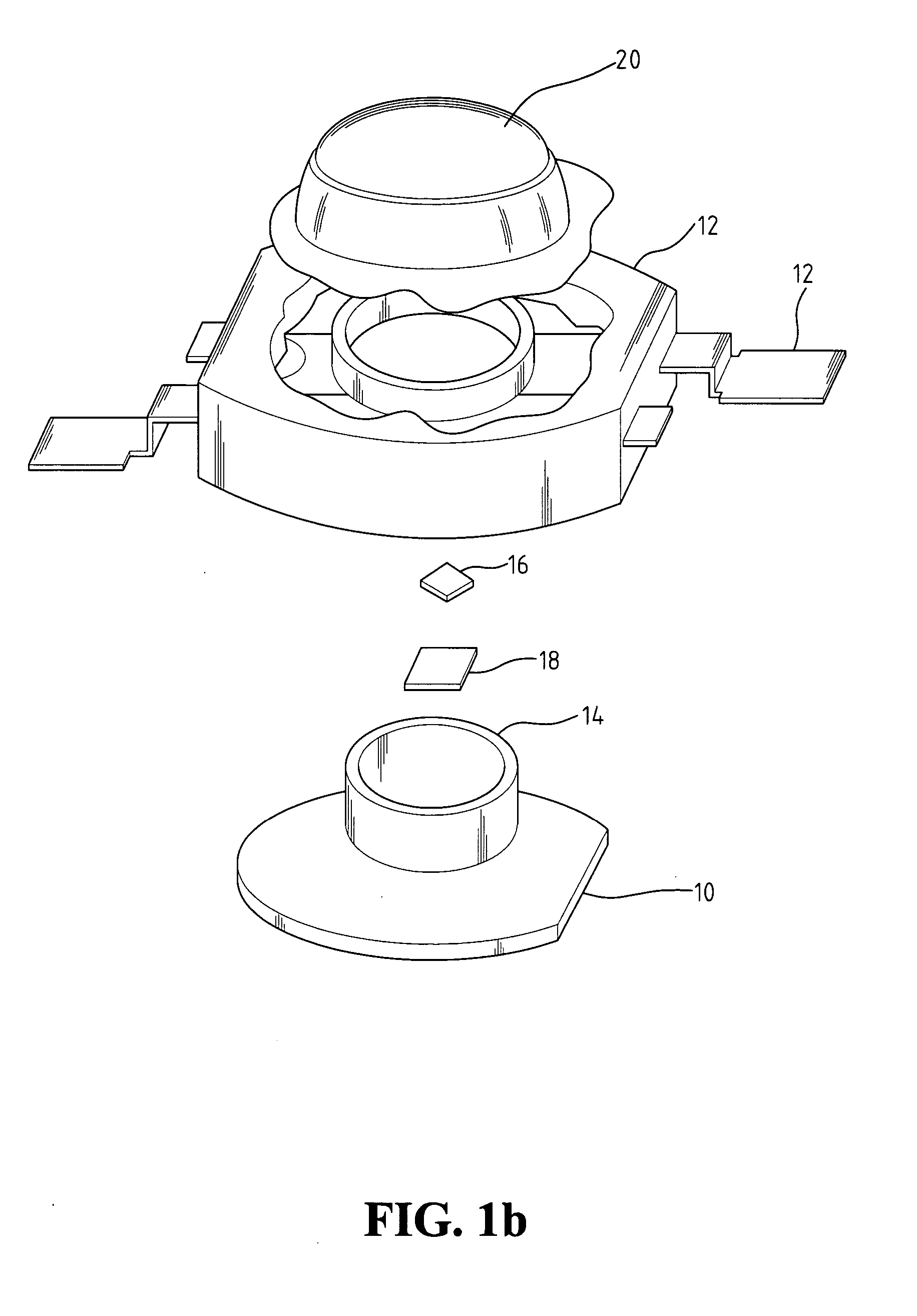
[0025]FIGS. 2a and 2b are schematic sectional view and blown-up view of the packaging structure according to the present invention. As illustrated, the packaging structure provided by the present embodiment contains at least a base 100, a reflection plate 110, the LED chip being packaged 150, a plurality of the bonding wires 120, and a transparent filler 130. The base 100, having a flat form factor, is composed of a heat sinking seat 102, a plurality of electrodes 104, and an insulator 106, integrated together into a single solid object. The heat sinking seat 102 and the electrodes 104 are made of a metallic material having high electrical and thermal conductivities. The insulator 106, on the other hand, is made of an insulating material such as resin or the like.

[0026] The heat sinking seat 102 is positioned in the middle of the flat base 100 with appropriate distances to the edges of the base 100. The heat sinking seat 102 is exposed both from the top surface of the base 100, and ...

second embodiment

[0028] The LED chip 150 is fixedly adhered to the top surface of the heat sinking seat 102 as mentioned earlier. The positive and negative electrodes (not shown) of the LED chip 150 are connected to separate electrodes 104 of the base 100 respectively via the bonding wires 120. As such, the heat produced by the LED chip is dissipated through the heat sinking seat 102 (i.e., the heat dissipation channel) while the bonding wires 120 and the electrodes 104 jointly provide access to the electricity (i.e., the electricity channel). With this separation of the electricity and heat dissipation channels, superior heat dissipation efficiency is thereby achieved. The through hole of the reflection plate 160 is filled with the filler 130 made of a transparent material such as resin so as to seal and protect the LED chip 150 and the bonding wires 120. In the present embodiment, the filler 130 completely fills up the through hole of the reflection plate 110. In a second embodiment as shown in FI...


PUM


Abstract

A packaging structure and a related fabrication method for high-power LED chip are provided herein, which mainly contains a base made of a metallic material and an electrically insulating material integrated into a single object. The metallic material forms a heat sinking seat in the middle of the base, which is exposed from the top surface of the base, and from the bottom surface or a side surface of the base. The metallic material also forms a plurality of electrodes surrounding the heat sinking seat, which are exposed from the top surface of the base, and from the bottom surface or a side surface of the base, respectively. The electrically insulating material is interposed between the electrodes and the heat sinking seat so that they are adhere together, and so that the heat sinking seat and any one of the electrodes, and any two electrodes are electrically insulated. The packaging structure achieves superior heat dissipation efficiency by separating the electricity and heat dissipation channels and, in another way, is applicable in mass production for a significantly reduced production cost.

Description

BACKGROUND OF THE INVENTION [0001] 1. Field of the Invention [0002] The present invention generally relates to light emitting diodes, and more particularly to a packaging structure for a high-power light emitting diode chip and a related fabrication method thereof. [0003] 2. The Prior Arts [0004] Spirited research activities have been focused on high-power light emitting diodes (LEDs) in the relevant industries in recent years. One of the most important considerations for the package of a high-power LED chip is about the appropriate handling of the high temperature and the heat produced by the high-power LED chip, so that the functionality, performance, and operational life of the LED chip is not compromised. [0005]FIG. 1a is a schematic sectional view showing a conventional packaging structure of a LED chip. As illustrated, the LED chip (or, some people refer to it as a LED die) 16 is positioned on top of a substrate 19 made of Bismaleimide Triazine (BT) resin. The electrodes (not ...

Claims


Application Information

Patent Timeline
Patent Type & Authority Applications(United States)
IPC IPC(8): H01L33/00H01L33/48H01L33/62H01L33/64
CPCH01L25/0753H01L33/486H01L33/62H01L33/642H01L2224/48091H01L2224/48247H01L2924/01079H01L2924/00014H01L2224/45144H01L2924/00H01L24/97H01L2224/8592H01L2224/48227H01L2924/12041H01L2924/181H01L2924/00012
Inventor LIN, CHENGSU, HUA-HSINNEI, MASAMI
Owner HIGH POWER LIGHTING CORP
Why Eureka
Try Eureka