Stacked type semiconductor memory device and chip selection circuit

Inactive Publication Date: 2007-06-07
PS4 LUXCO SARL
View PDF31 Cites 63 Cited by
  • Summary
  • Abstract
  • Description
  • Claims
  • Application Information

AI Technical Summary

Benefits of technology

[0023] As described above, according to the present invention, in order to select a desired semiconductor chip based on chip identification numbers different from each other in a stacked type semiconductor device in which a plurality of semiconductor chips is stacked, a structure is employed in which an operation circuit and a comparison circuit are provided corresponding to each semiconductor chip, the plurality of identification numbers is generated based on a plurality of operation circuits connected in cascade, and the comparison circuit detects its equality with a common chip selection address. By emp

Problems solved by technology

Construction of the semiconductor memory using a single semiconductor chip requires finer microfabrication and the yield deteriorates.
However, in such a structure, it is necessary to separately form the connection paths for the selection sig

Method used


Image

  • Stacked type semiconductor memory device and chip selection circuit
  • Stacked type semiconductor memory device and chip selection circuit
  • Stacked type semiconductor memory device and chip selection circuit

Examples


Example

[0034] Embodiments of the invention will be described below with reference to accompanying drawings. In this embodiment, a stacked type semiconductor memory device having a plurality of stacked DRAM chips will be described as an example of a stacked type semiconductor device to which the present invention is applied.

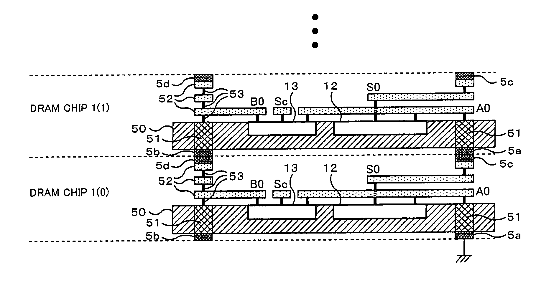
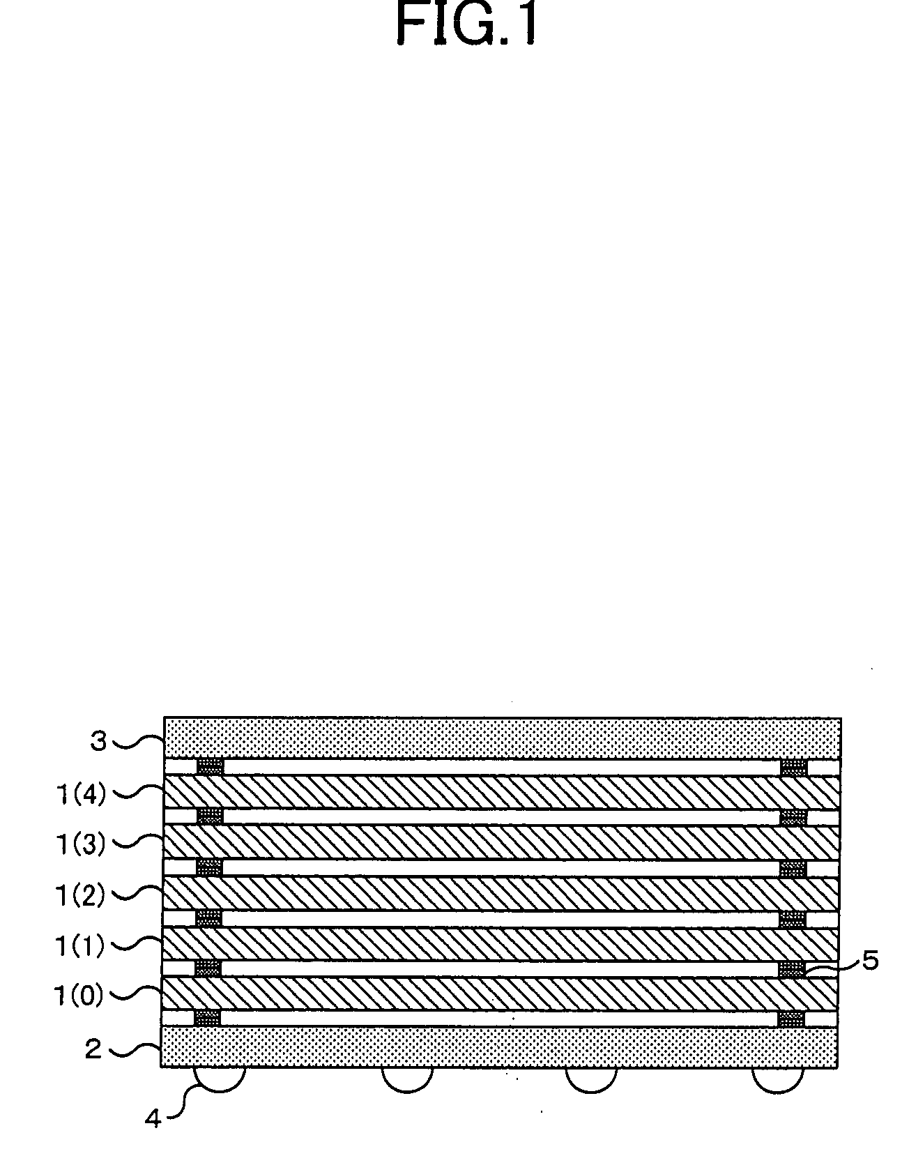
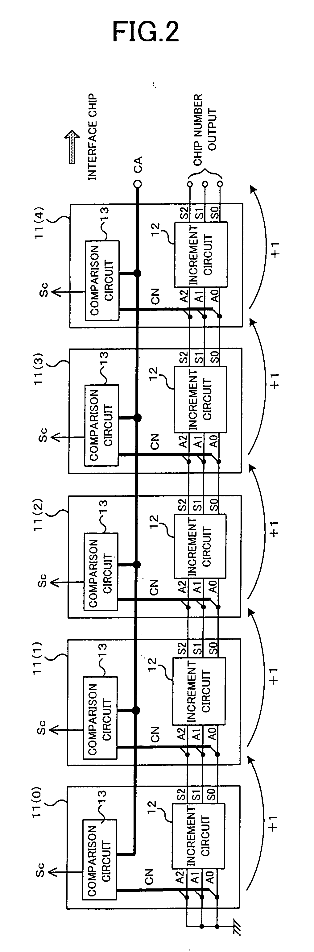
[0035]FIG. 1 is a diagram showing an example of a cross-sectional structure of the stacked type semiconductor memory device of this embodiment. The semiconductor memory device shown in FIG. 1 has a structure in which DRAM chips 1 are stacked in five layers over an interposer board 2 of the lowest layer and an interface chip 3 is stacked thereon. Respective DRAM chips 1 of the first to fifth layers are distinguished from each other by denoting numbers in parenthesis such as DRAM chip 1(0), 1(1), 1(2), 1(3), 1(4) successively.

[0036] The five-layer DRAM chips 1(0) to 1(4) have the same storage capacity and the same structure and can perform read / write operation by accessi...


PUM


Abstract

A stacked type semiconductor memory device of having a structure in which a plurality of semiconductor chips is stacked and a desired semiconductor chip can be selected by assigning a plurality of chip identification numbers different from each other are individually assigned to the plurality of semiconductor chips comprising: a plurality of operation circuits which is connected in cascade in a stacking order of the plurality of semiconductor chips and outputs the plurality of identification numbers different from each other by performing a predetermined operation; and a plurality of comparison circuits which detects whether or not each the identification number and a chip selection address commonly connected to each the semiconductor chip are equal to each other by comparing them.

Description

BACKGROUND OF THE INVENTION [0001] 1. Field of the Invention [0002] This invention relates to a semiconductor device having a structure in which a plurality of semiconductor chips is stacked and a specific semiconductor chip can be selected, and particularly relates to a semiconductor device in which a unique identification number is assigned to each semiconductor chip in order to select a specific semiconductor chip. [0003] 2. Description of the Related Art [0004] Recently, an increase in storage capacity is required for semiconductor memories such as DRAMs. Construction of the semiconductor memory using a single semiconductor chip requires finer microfabrication and the yield deteriorates. Therefore, a stacked type semiconductor device having a structure in which a plurality of semiconductor chips is stacked has been proposed. For example, by employing a 3 dimensional structure in which a plurality of semiconductor chips of the same type is stacked in multiple layers, a small stac...

Claims


Application Information

Patent Timeline
IPC IPC(8): H01L23/02
CPCG11C5/02G11C5/04G11C2029/4402H01L25/0657H01L2224/16145H01L2225/06513H01L2924/15311H01L2924/01021
Inventor YAMADA, JUNJIIKEDA, HIROAKISHIBATA, KAYOKOINOUE, YOSHIHIKOMIWA, HITOSHIIJIMA, TATSUYA
Owner PS4 LUXCO SARL
Why Eureka
Try Eureka