Supercharge Your Innovation With Domain-Expert AI Agents!

Data input circuit of semiconductor memory device and data input method thereof

a data input circuit and data input technology, applied in the field can solve the problems of data input margins that cannot be secured stably, and the reduction of data input margins may generate write operation failures of semiconductor memory devices, and achieve the effect of ensuring stably the data input margin

Inactive Publication Date: 2007-06-07
CONVERSANT INTPROP MANAGEMENT INC
View PDF5 Cites 13 Cited by
  • Summary
  • Abstract
  • Description
  • Claims
  • Application Information

AI Technical Summary

Benefits of technology

[0021] An embodiment of the present invention is that it provides a data input circuit of a semiconductor memory device, in which it can secure a data input margin stably by controlling an operating start point of the sense amplifier circuit based on the data strobe signal.
[0022] Another embodiment of the present invention is that it provides a data input method of a semiconductor memory device, in which it secure a data input margin stably by controlling an operating start point of the sense amplifier circuit based on the data strobe signal.

Problems solved by technology

Accordingly, a problem arises because data input margin cannot be secured stably.
The reduction in the data input margin may generate write operation fail of the semiconductor memory devices.

Method used


Image

  • Data input circuit of semiconductor memory device and data input method thereof
  • Data input circuit of semiconductor memory device and data input method thereof
  • Data input circuit of semiconductor memory device and data input method thereof

Examples


Embodiment Construction

[0034] The present invention will now be described in detail in connection with certain exemplary embodiments with reference to the accompanying drawings.

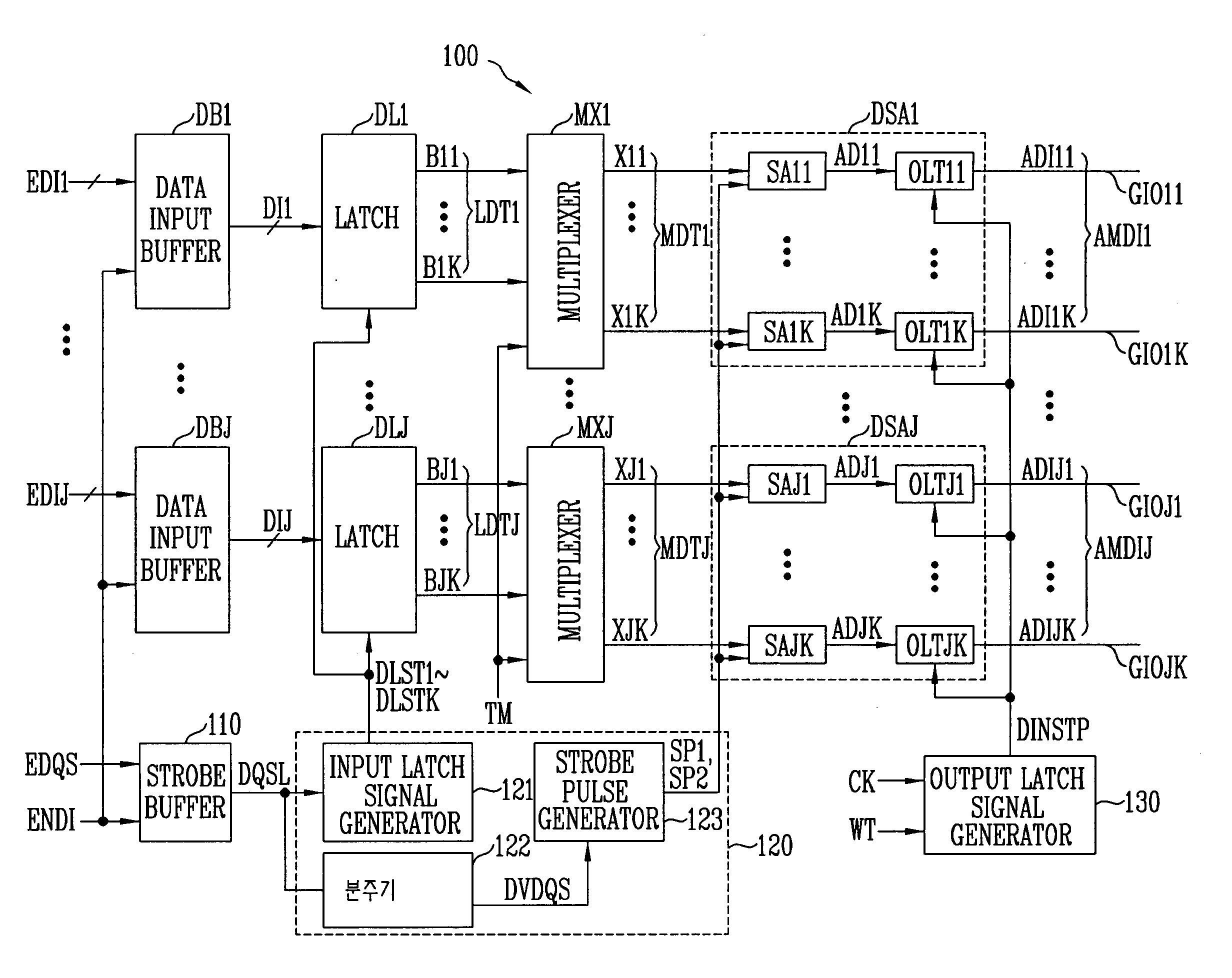
[0035]FIG. 3 is a schematic block diagram of a data input circuit of a semiconductor memory device according to an embodiment of the present invention.

[0036] Referring to FIG. 3, a data input circuit 100 includes a strobe buffer 110, an input controller 120, an output latch signal generator 130, data input buffers DB1 to DBJ (J is an integer), latches DL1 to DLJ, multiplexers MX1 to MXJ, and data sense amplifiers DSA1 to DSAJ.

[0037] The strobe buffer 110 receives an external data strobe signal EDQS in response to a data input signal ENDI and outputs a data strobe signal DQSL. In more detail, the strobe buffer 110 converts a voltage level of the external data strobe signal EDQS into a CMOS logic level (i.e., a voltage level suitable for the operation of the input controller 120) and outputs the data strobe signal DQSL having a co...


PUM


Abstract

A data input circuit of a semiconductor memory device and a data input operating method thereof, in which data input margin can be secured. The data input circuit includes a strobe buffer that receives an external data strobe signal in response to a data input signal and outputs a data strobe signal, data input buffers that receive external input data, respectively, in response to the data input signal and output input data, respectively, an input controller that generates input latch signals and strobe pulse signals based on the data strobe signal, an output latch signal generator that generates an output latch signal in response to a clock signal and a write instruction, latches that latch the input data, respectively, in response to the input latch signals and output latch data, respectively, multiplexers that receive the latch data, respectively, and output multiplexed data, respectively, and data sense amplifiers that sense and amplify the multiplexed data, respectively, in response to the strobe pulse signals and output amplified data to global I / O lines, respectively, in response to the output latch signal.

Description

BACKGROUND [0001] 1. Field of the Invention [0002] The present invention generally relates to semiconductor memory devices, and more particularly, to a data input circuit of a semiconductor memory device. [0003] 2. Discussion of Related Art [0004] In general, a data input circuit of a semiconductor memory device receives input data from an external device in synchronization with a data strobe signal. As described above, the data input circuit further receives the data strobe signal other than the externally input data from the external device. [0005]FIG. 1 is a schematic block diagram of a data input circuit, a data output circuit, and an internal circuit of a semiconductor memory device in the related art. [0006] Referring to FIG. 1, a data input circuit 10 and a data output circuit 30 are connected to an internal circuit 20 through a Global Input and Output (GIO) line 40. Though not shown in FIG. 1, the internal circuit 20 includes a core circuit having memory cells. FIG. 1 shows ...

Claims


Application Information

Patent Timeline
IPC IPC(8): G11C7/10
CPCG11C7/1078G11C7/1084G11C7/1087G11C7/1093G11C29/02G11C29/022G11C29/50G11C29/50012G11C7/10
Inventor CHA, JAE HOON
Owner CONVERSANT INTPROP MANAGEMENT INC
Features
  • R&D
  • Intellectual Property
  • Life Sciences
  • Materials
  • Tech Scout
  • Unparalleled Data Quality
  • Higher Quality Content
  • 60% Fewer Hallucinations
Learn More