Defect inspection method, defect inspection system, defect inspection program, and memory medium with that program memorized in it

a technology of defect inspection and inspection method, applied in the direction of character and pattern recognition, instruments, computing, etc., can solve the problems of difficult application of defects to reject detection operations, publications that are not designed to detect defects at the wafer edge portion, and the cracking of the wafer, so as to reduce the operating time and tact time , the effect of short inspection tim

Inactive Publication Date: 2007-06-07
AVIS CORP
View PDF2 Cites 14 Cited by
  • Summary
  • Abstract
  • Description
  • Claims
  • Application Information

AI Technical Summary

Benefits of technology

[0012] One object of the present invention is to provide a defect inspection method, a defect inspection system, and a defect inspection program, which enables an inspection...

Problems solved by technology

In particular, the presence of cracks on a wafer edge portion will often cause the wafer to crack apart.
However, both methods of these publications are not designed to detect defects at the wafer edge portion, especially the edge cut line width, although they may be used to detect the wafer edge portion.
For this reason, it is difficult to apply them to rejects detection operation at the steps subsequent to the photoresist thin film coating.
However, each of those techniques renders detection of defects all around the periphery of the edge portion difficult, because it is not designed to pick up the edge image all around the periphery.
However, computation of enormous volumes of data must be implemented for such image data comparison, and some considerable amount of processing time would be taken ev...

Method used


Image

  • Defect inspection method, defect inspection system, defect inspection program, and memory medium with that program memorized in it
  • Defect inspection method, defect inspection system, defect inspection program, and memory medium with that program memorized in it
  • Defect inspection method, defect inspection system, defect inspection program, and memory medium with that program memorized in it

Examples


Embodiment Construction

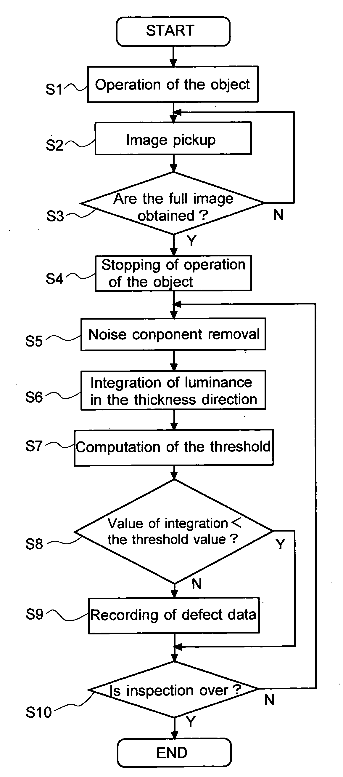
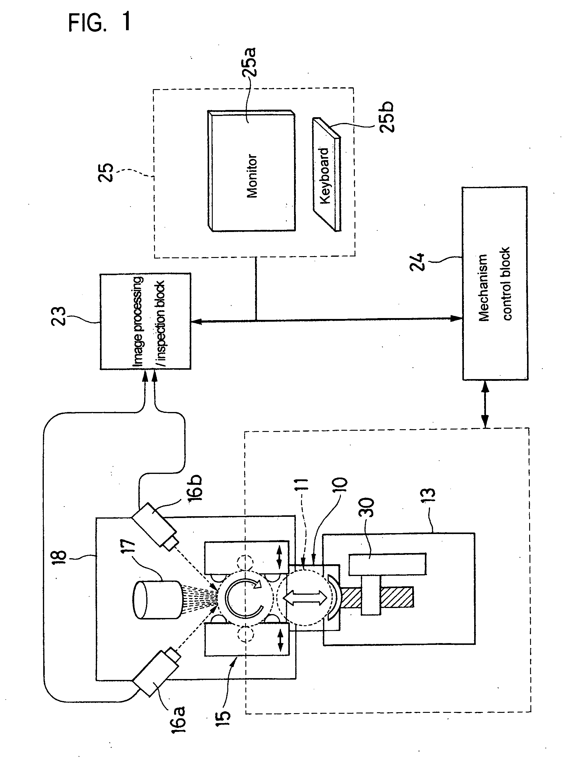
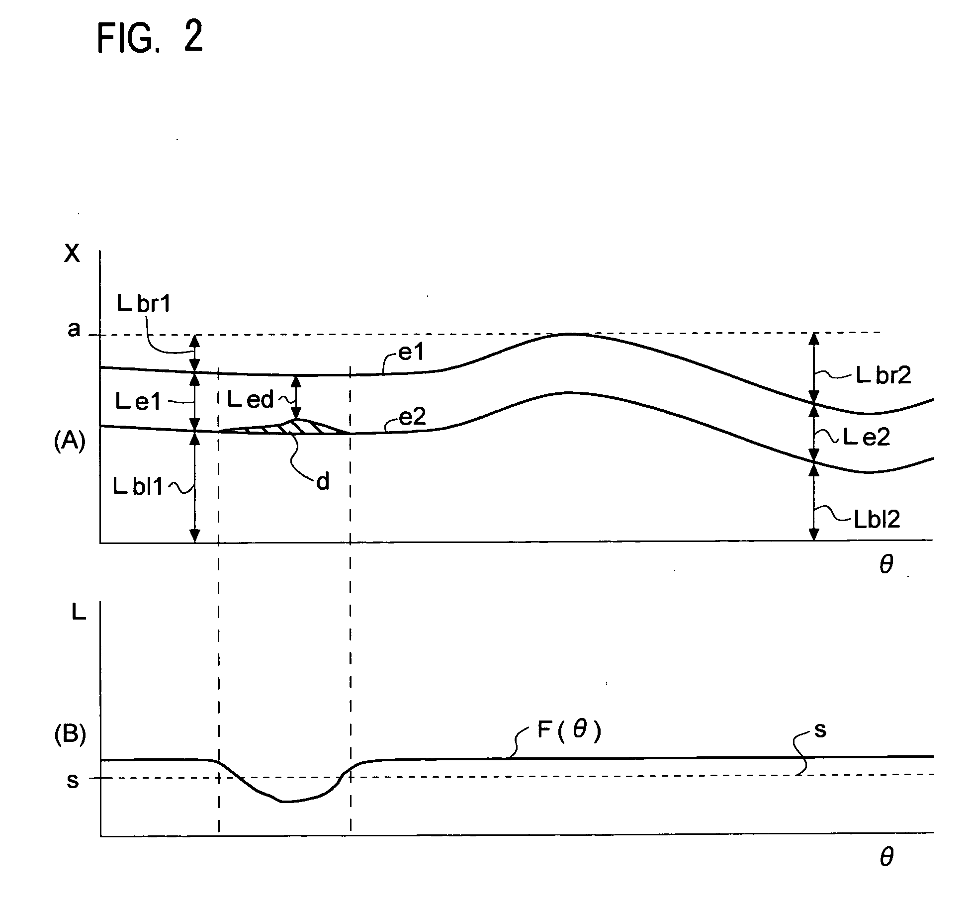
[0027] The defect inspection method of the present invention involves summation of the luminance and the number of pixels in the widthwise direction of the image of the object to be inspected, said object being identifiable as a linear or band-like one, so that the object is determined as defective when the value of summation is below the given reference value.

[0028] Thus, if the luminance and the number of pixels of the image of the object to be inspected in its widthwise direction orthogonal to its longitudinal direction, wherein the object is identifiable as a linear or band-like one, are summated up, it is then possible to make inspection of defects very easily and very quickly. That is, when the object to be inspected is of constant quality, the summation of the luminance and the number of pixels of the object to be inspected in the widthwise direction becomes equal. When there is a defect, however, the value of summation of the luminance and the number of pixels in the widthw...


PUM


Abstract

The object of the invention is to provide a defect inspection method, a defect inspection system, and a defect inspection program, in which the inspection time for the object to be inspected and identifiable as a linear or band-like one is so very short that the operation time and tact time can be cut down, and which prevents misidentification even when there is distortion or deformation in the object, thereby making precise defect inspection possible. In the defect inspection method, system and program, the luminance and the number of pixels in the widthwise direction of the image of the object to be inspected such as the edge portion of a semiconductor wafer, wherein the image is identifiable as a linear or band-like one, are summated up, and the object is determined as defective when the value of the summation is below a reference value.

Description

BACKGROUND OF THE INVENTION [0001] 1. Art Field [0002] The present invention relates to a defect inspection method, a defect inspection system and a defect inspection program, all adapted to detect defects such as flaws, stains, dusts, and cracks in and on, for instance, the outer peripheries of semiconductor wafers (hereinafter called the wafer edges), the outer peripheries of disks such as hard disks, and electric wires, optical fibers, etc. which are imaged in a linear form. [0003] 2. Background Art [0004] Generally, defect inspection is carried out, for instance, at the time of supplying industrial products to the market or passing them into another process for removal of defective products. For instance, in semiconductor fabrication processes, defect inspection is performed for each fabrication step. [0005] A main object of this defect inspection is to make inspection of defects such as flaws and cracks on the surfaces of, for instance, semiconductor wafers as well as dusts and...

Claims


Application Information

Patent Timeline
IPC IPC(8): G06K9/00
CPCG06K9/00G06K2209/19G06V2201/06G06F18/00
Inventor KOSHIKAWA, KAZUNORI
Owner AVIS CORP
Why Eureka
Try Eureka