Liquid crystal display device and inspecting method thereof

a display device and liquid crystal technology, applied in static indicating devices, non-linear optics, instruments, etc., can solve the problems of defective pixels being inspected, adversely affected by the production cost of the substrate, and long measuring time, etc., to achieve short inspection time and high accuracy

Inactive Publication Date: 2007-06-05
SONY CORP
View PDF8 Cites 3 Cited by
  • Summary
  • Abstract
  • Description
  • Claims
  • Application Information

AI Technical Summary

Benefits of technology

[0016]Therefore, an object of the present invention is to provide a liquid crystal display device and an inspecting method that allow pixels to be inspected for defective ones with a digital signal in a short inspecting time and a high accuracy without the influence of parasitic capacitances of data signal lines and an evaluating system.
[0022]Unlike a method for evaluating an analog waveform, according to the present invention, defective pixels can be detected with a digital signal. Thus, a system that accurately evaluates a detected analog waveform is not required. In addition, without the influence of deviations of a parasitic capacitance of data signal lines and a capacitance of a tester system, pixels can be accurately inspected for defective ones.

Problems solved by technology

Thus, the production cost of the substrate adversely becomes high.
However, in such methods, since a liquid crystal display device is actually driven and an image is displayed thereon, defective pixels are inspected.
Thus, a long measuring time is required and high productivity cannot be expected.
This is because from view point of cost, it is not practical to remove liquid crystal the liquid crystal display device, correct the defective pixels, and then fill the liquid crystal in the liquid crystal display device.
However, according to the method described in the related art reference (patent document 1), since defective pixels are evaluated one by one, when a high resolution liquid crystal display panel having more than 1,000,000 and 2,000,000 pixel such as (1280×1024) and (1920×1200), is evaluated for defective pixels, it takes a long measuring time to evaluate all the pixels.
In addition, the parasitic capacitances deviate for each LCD panel.
As a result, without careful consideration of a parasitic capacitance of data signal lines and a capacitance of the tester, capacitances of pixels cannot be accurately evaluated with detected values.

Method used


Image

  • Liquid crystal display device and inspecting method thereof
  • Liquid crystal display device and inspecting method thereof
  • Liquid crystal display device and inspecting method thereof

Examples


first embodiment

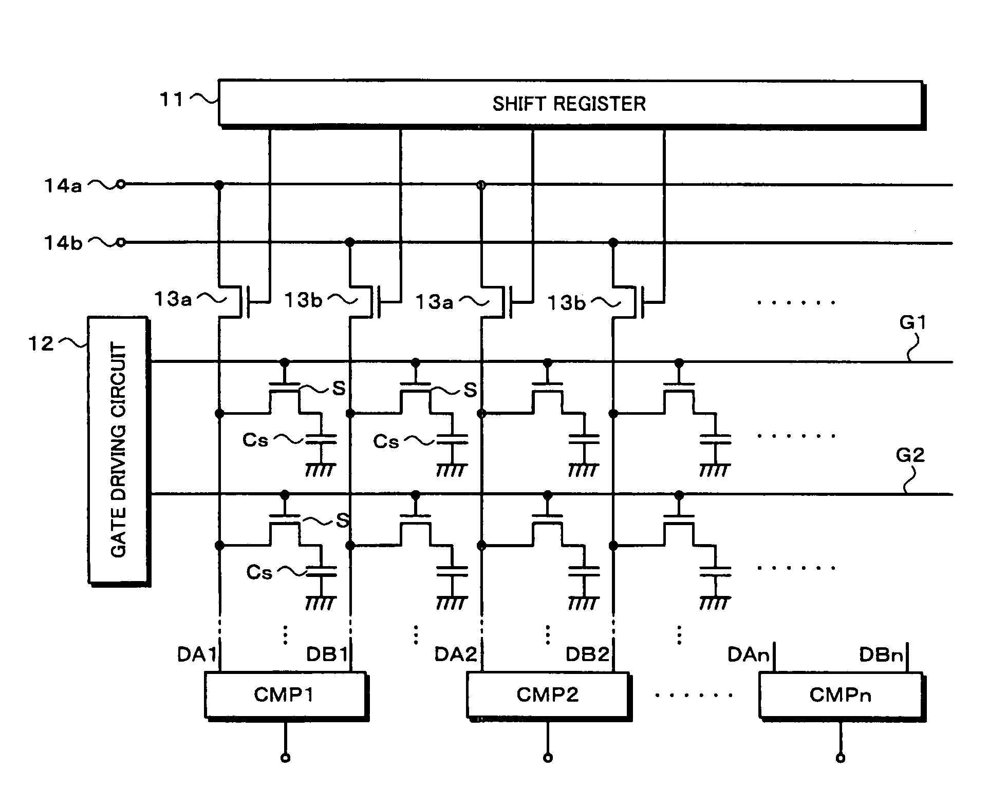
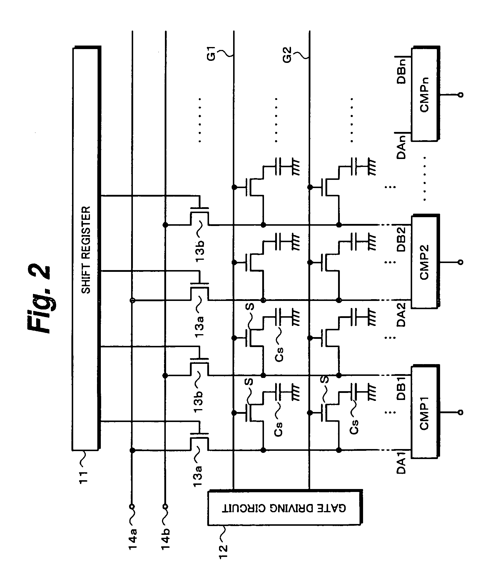
[0037]FIG. 2 shows a structure of an embodiment of the present invention. Reference numeral 11 represents a shift resistor that operates as a horizontally-scanning circuit. Reference numeral 12 represents a gate driving circuit that operates as a vertically-scanning circuit. When the number of pixels is represented by (H×V), H data signal lines and V gate signal lines are disposed. Each of the pixel portions is disposed at each of the intersections of the data signal lines and the gate signal lines. Each of the pixel portions is composed of a pixel transistor S and a capacitor Cs. A pixel electrode is connected to a capacitor Cs in parallel. Liquid crystal is sealed between a pixel electrode and an opposite electrode.

[0038]In the structure shown in FIG. 2, two adjacent pixels are activated at a time. In other words, drains of odd-numbered transistors 13a are connected to one input signal terminal 14a. On the other hand, drains of even-numbered transistors 13b are connected to anothe...

second embodiment

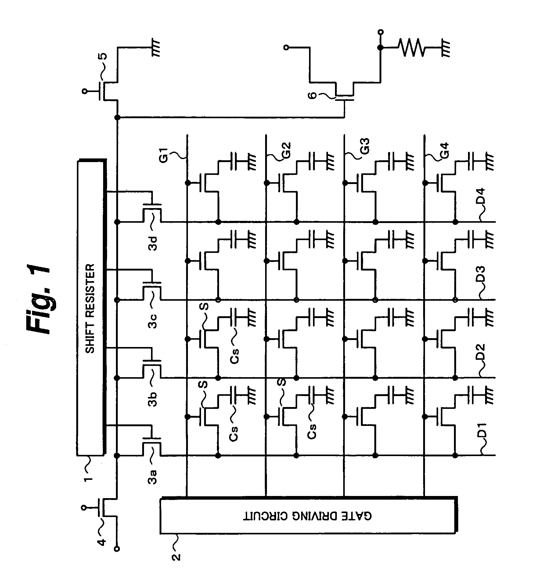
[0065]FIG. 10 shows another embodiment (second embodiment) of the present invention. For simplicity, in FIG. 10, similar portions to those in FIG. 2 will be denoted by similar reference numerals. In the second embodiment, signal voltages are not written to a plurality of pixels in parallel. Instead, a signal voltage is written to pixels one by one. Thus, there are h data lines D1 to Dh. There are v gate signal lines G1 to Gv. A signal voltage is applied to an input terminal 14. When one transistor 13 is turned on, the voltage is written thereto in a point sequence.

[0066]In the second embodiment, auxiliary data signal lines D1′ to Dn′ are disposed in parallel with the data signal lines D1 to Dn, respectively. Each of connected points of pixel transistors S and capacitors Cs of pixel portions is connected to the auxiliary data signal lines D1′ to Dn′. In addition, as shown in FIG. 11, AND gates AN11 to ANvh are disposed corresponding to all the pixels. A voltage of the auxiliary data ...


PUM

PropertyMeasurementUnit
voltagesaaaaaaaaaa
areaaaaaaaaaaa
non-defect rateaaaaaaaaaa

Abstract

Output signals of two adjacent data signal lines DA1 to DAn and DB1 to DBn are supplied to comparators CMP1 to CMPn, respectively. When pixels are inspected, different signal potentials are input to signal input terminals 14a and 14b. Signals are written to pixels from the first row to the last row. Thereafter, a pre-charging process is performed by supplying a voltage to the terminals 14a and 14b. Thereafter, signals are read from all the pixels from the first row to the last row. The signal potentials that have been read are compared by the comparators CMP1 to CMPn. Depending on the relations of voltages written as digitally-compared outputs of the comparators CMP1 to CMPn, defective pixels are detected.

Description

BACKGROUND OF THE INVENTION[0001]1. Field of the Invention[0002]The present invention relates to a liquid crystal display device for use with an active-matrix-type liquid crystal display device and an inspecting method thereof, in particular, an inspecting method for inspecting defective pixels on a substrate.[0003]2. Description of the Related Art[0004]In an active-matrix-type liquid crystal display device, switching thin film transistors (TFT) and transparent electrodes are disposed at intersections of data signal lines and gate signal lines so as to control voltages of the transparent electrodes. For example, Si-type liquid crystal display panels that are small and have high resolutions are being increasingly used for cellular phone units, personal digital assistants (PDA), and so forth.[0005]A Si-type liquid crystal display panel is structured in such a manner that liquid crystal is sealed between a large scale integrated circuit (LSI), on which a transistor, a capacitor, and a ...

Claims


Application Information

Patent Timeline
Patent Type & Authority Patents(United States)
IPC IPC(8): G09G3/36G02F1/13G02F1/1368G09G3/00
CPCG09G3/006G09G3/3648G09G2330/08
Inventor ISHIKAWA, KENICHIROTAKITA, HISASHIYOSHIDA, JOE
Owner SONY CORP
Why Eureka
Try Eureka