Microscope for inspecting semiconductor wafer

a microscope and semiconductor wafer technology, applied in the direction of microscopes, semiconductor/solid-state device testing/measurement, instruments, etc., can solve the problems of complicated process, difficult removal of remaining layers of semiconductor wafer, and difficulty in removing portions of semiconductor wafers, etc., to achieve the effect of increasing the manufacturing yield

Inactive Publication Date: 2005-05-24
SAMSUNG ELECTRONICS CO LTD
View PDF17 Cites 4 Cited by
  • Summary
  • Abstract
  • Description
  • Claims
  • Application Information

AI Technical Summary

Benefits of technology

[0013]To overcome the problems described above, preferred embodiments of the present invention provide a microscope for inspecting a semiconductor wafer that can perform a precise inspection and clearly analyze or clarify defect factors, thereby increasing a manufacturing yield.
[0014]It is another object of the present invention to provide a microscope for inspecting a semiconductor wafer with a short inspection time.

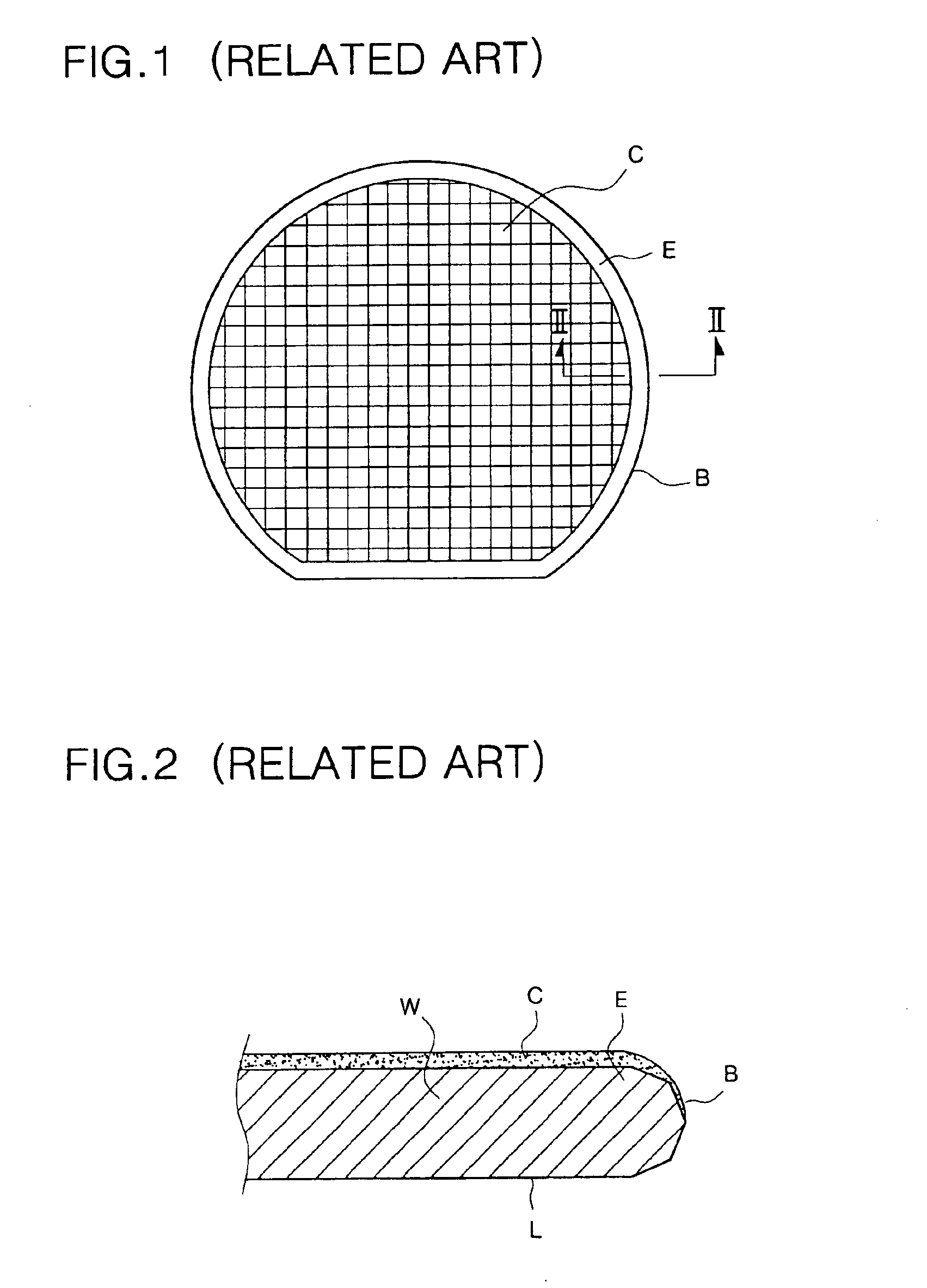
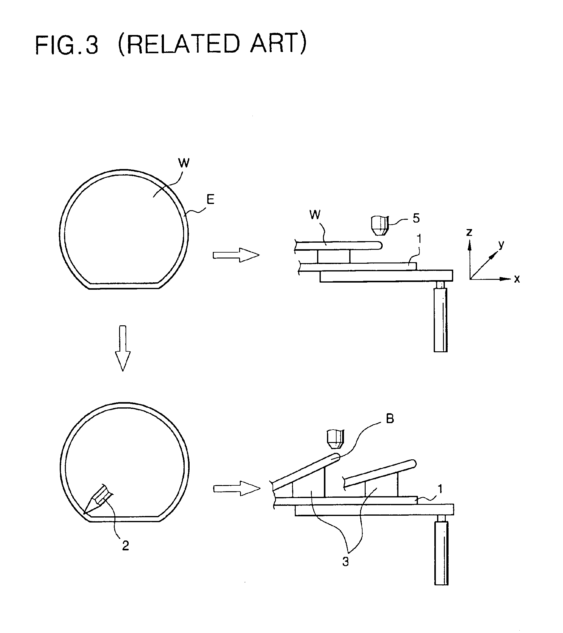
Problems solved by technology

As a semiconductor device is highly-integrated, layers formed on a semiconductor wafer become diverse, and remaining layers on an edge portion and a portion having a predetermined thickness (hereinafter, referred to as bevel portion) of the semiconductor wafer become more difficult to remove.
However, this has a problem in that a process is complicated and cannot solve a fundamental level of defects resulting from the edge portion and the bevel portion of the semiconductor wafer.
First, since the sample piece stage just performs a horizontal shift and a vertical shift, it is impossible to simultaneously inspect the edge portion and the bevel portion of the semiconductor wafer, thereby increasing the wafer inspection time.
Second, during handling of a wafer sample piece, such as conveying and cutting a defective semiconductor wafer, other contamination of the wafer sample piece can occur, whereupon the inspection data can have errors.
Third, since regular monitoring is not performed during a process of manufacturing the semiconductor wafer, it is difficult to find and prevent defects in advance.
Finally, it is difficult to precisely inspect the semiconductor wafer having defects in the edge portion and the bevel portion and to clearly analyze or clarify defect factors, and also the inspection time is long, such that an appropriate remedy cannot be performed.

Method used


Image

  • Microscope for inspecting semiconductor wafer
  • Microscope for inspecting semiconductor wafer
  • Microscope for inspecting semiconductor wafer

Examples


Embodiment Construction

[0031]Reference will now be made in detail to preferred embodiments of the present invention, examples of which is illustrated in the accompanying drawings.

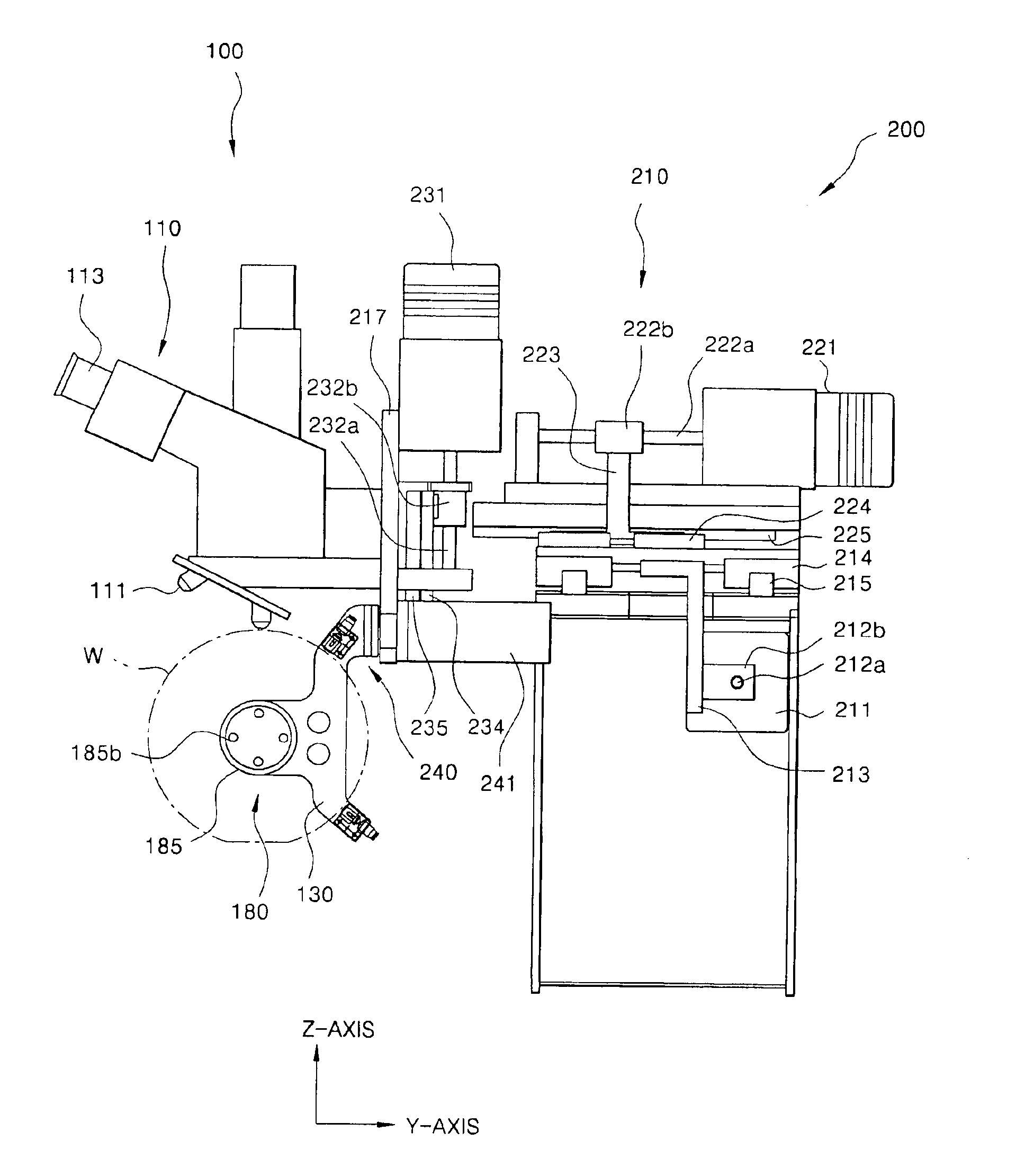
[0032]FIG. 6 is a schematic view illustrating a wafer probing system employing a microscope for probing a semiconductor wafer. FIG. 7 is a front view illustrating the microscope of FIG. 6, and FIG. 8 is a side view illustrating the microscope of FIG. 6.

[0033]The microscope 100 includes an optical unit 110, a display unit 120, a sample piece stage 130, a controller 170, a rotation unit 180, and a stage moving unit 200.

[0034]The optical unit 110 includes an objective lens 111 and an ocular 113, and is used to observe a wafer sample piece laid on the sample piece stage 130 through the objective lens 110 and the ocular 113. The display unit 120 magnifies and displays an image of the sample piece wafer observed by the optical unit 110. The rotation unit 180 rotates the sample piece wafer on the sample piece stage 130 to a horizontal d...


PUM


Abstract

A microscope for inspecting a semiconductor wafer includes an optical unit including objective lenses and oculars for observing the semiconductor wafer; a display unit for magnifying and displaying an image of the semiconductor wafer observed by the optical unit; a sample piece stage holding the semiconductor wafer; a stage moving unit for moving the semiconductor wafer in an x-axis direction, a y-axis direction or a z-axis direction; a stage rotation unit for rotating the semiconductor wafer in a horizontal direction; a stage tilting unit for tilting the semiconductor wafer; and a controller for controlling operation of the microscope.

Description

CROSS REFERENCES TO RELATED APPLICATIONS[0001]This application claims the benefit under 35 U.S.C. § 119 of Korean Patent Application No. 2001-14093 filed on Mar. 19, 2001 the entirety of which is hereby incorporated by reference for all purposes as if fully set forth herein.BACKGROUND[0002]1. Field of the Invention[0003]The present invention relates to a microscope for inspecting a semiconductor wafer.[0004]2. Description of Related Art[0005]As a semiconductor device is highly-integrated, layers formed on a semiconductor wafer become diverse, and remaining layers on an edge portion and a portion having a predetermined thickness (hereinafter, referred to as bevel portion) of the semiconductor wafer become more difficult to remove. Such remaining layers on the edge portion and the bevel portion of the semiconductor wafer are transited to a chip portion of the semiconductor wafer during a dry-etching process and a wet-etching process and serve as particles that cause various defects of...

Claims


Application Information

Patent Timeline
Patent Type & Authority Patents(United States)
IPC IPC(8): G02B21/00G02B21/24G02B21/26H01L21/66
CPCG02B21/26G02B21/0016H01L22/00
Inventor WOO, JAI YOUNGKIM, KYUNG DAEKIM, JIN SUNGLEE, YOUNG GOO
Owner SAMSUNG ELECTRONICS CO LTD
Why Eureka
Try Eureka