System for controlling semiconductor device manufacturing process and method of controlling semiconductor device manufacturing process

a semiconductor device and manufacturing process technology, applied in the direction of program control, total factory control, instruments, etc., can solve the problems of deterioration of consumable components, difficulty in maintaining wafer quality constant, and managing the maintaining of the state of the semiconductor manufacturing apparatus in the semiconductor device manufacturing process

Inactive Publication Date: 2007-06-07
FUJITSU LTD
View PDF6 Cites 15 Cited by
  • Summary
  • Abstract
  • Description
  • Claims
  • Application Information

AI Technical Summary

Benefits of technology

[0024] In the system for controlling a semiconductor device manufacturing process according to this aspect, the alternative recipe to be returned to the manufacturing management system is prepared beforehand inside the manufacturing process control system. Thus, even in the case where an optimum recipe cannot be derived, it does not happen that a recipe cannot be returned to the manufacturing management system, and the semiconductor manufacturing apparatus is not stopped. Accordingly, device manufacture and device quality are not adversely affected.
[0025] According to another aspect

Problems solved by technology

In recent years, smaller-size, higher-density semiconductor devices are being demanded, and it is becoming difficult to maintain wafer quality constant and manage the maintaining of the state of a semiconductor manufacturing apparatus in a semiconductor device manufacturing process.
However, in an actual manufacturing step, if the sizes of semiconductor devices are reduced and the densities thereof are increased, the semiconductor devices are not necessarily processed under a condition in which a semiconductor manufacturing apparatus is stable.
Generally, when a semiconductor manufacturing apparatus is operated for a long time, adjusted values thereof are changed, and consumable components are deteriorated.
However, even in the case where such a system is used, it has revealed that the following inconveniences occ

Method used


Image

  • System for controlling semiconductor device manufacturing process and method of controlling semiconductor device manufacturing process
  • System for controlling semiconductor device manufacturing process and method of controlling semiconductor device manufacturing process
  • System for controlling semiconductor device manufacturing process and method of controlling semiconductor device manufacturing process

Examples


first embodiment

(1) First Embodiment

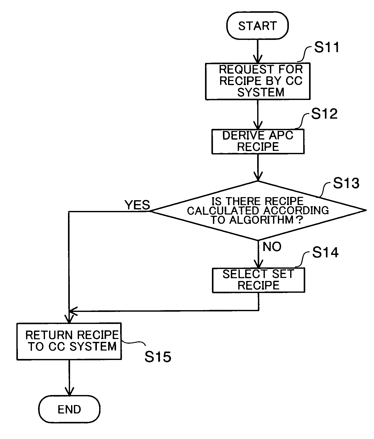
[0042] In a first embodiment, first, an overview of a semiconductor device manufacturing system will be described. Next, a description will be given of the derivation of an APC recipe for preventing a CIM system from stopping. Then, a description will be given of a method of controlling a semiconductor device manufacturing process for preventing the CIM system from stopping.

(Overview of Semiconductor Device Manufacturing System)

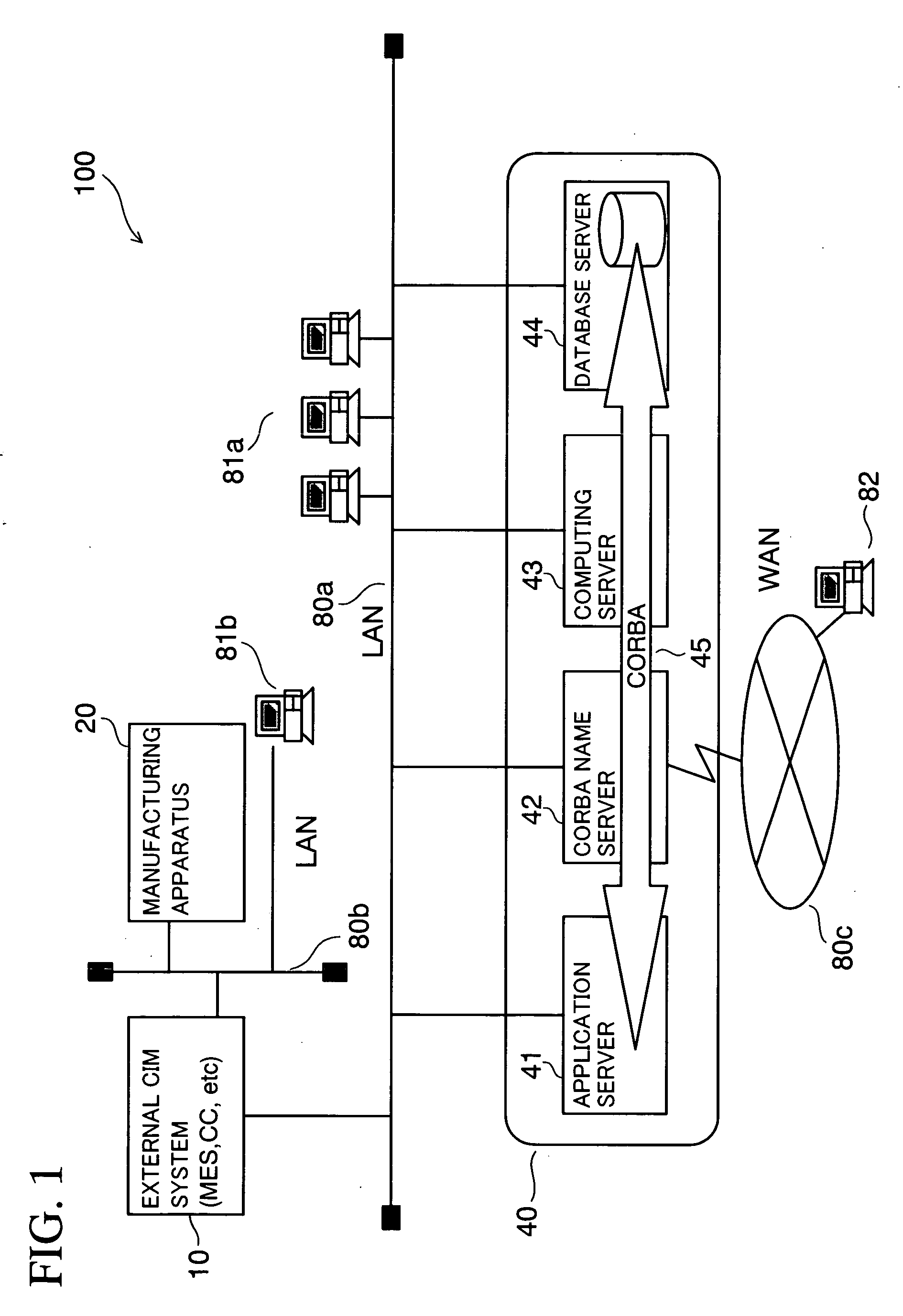
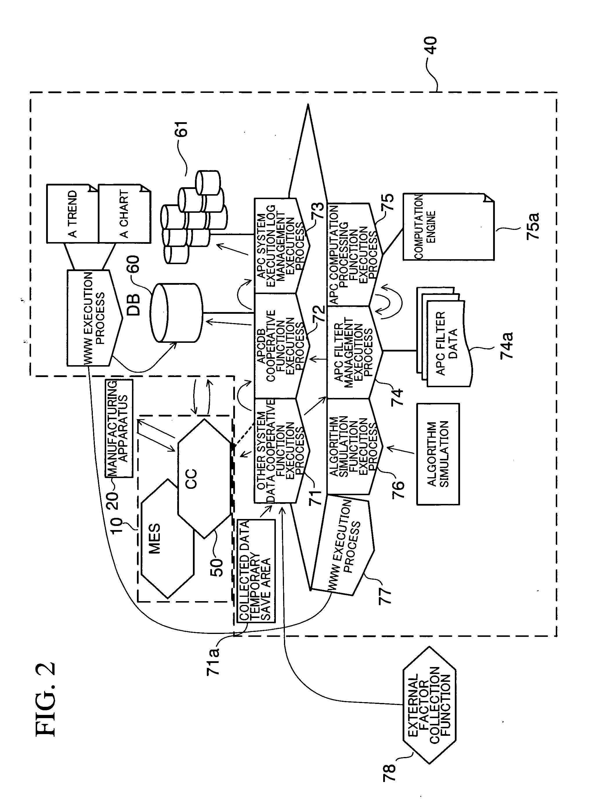
[0043]FIG. 1 is a schematic configuration diagram showing one example of a semiconductor device manufacturing system 100. The semiconductor device manufacturing system 100 includes an APC system 40, an external CIM system 10, and a manufacturing apparatus 20 as basic components.

[0044] The APC system 40 includes an application server 41, a Common Object Request Broker Architecture (CORBA) name server 42, a computing server 43, and a database server 44.

[0045] The application server 41 stores application programs for realizing processing...

second embodiment

(2) Second Embodiment

[0108] In the first embodiment, even in the case where an optimum APC recipe is not derived in the APC system 40, a recipe is selected to be returned to the CC system 50 by preparing recipes beforehand. In a second embodiment, a specific method of selecting a recipe is specified. The configuration of a semiconductor device manufacturing system 100 used in this embodiment is the same as that described in the first embodiment.

[0109]FIG. 11 is a view showing one example of a response recipe management table for the case where the derivation of an APC recipe has failed. Data in the first row indicate that as a result of performing an APC calculation using algorithm m-001, an algorithm value (recipe value) has not been obtained. That is, the following situation is indicated: when apparatus information and the like are obtained from the CC system 50 and a computation of a recipe value is performed using a predetermined algorithm, a recipe value cannot be derived for ...

third embodiment

(3) Third Embodiment

[0136] In a third embodiment, a data communication method between the APC system 40 and the CC system 50 will be described.

[0137] Here, referring to FIGS. 14 and 15, a description will be given by taking as an example the case where the APC system 40 cooperates with the CC system 50 and where the CC system 50 inquires of the APC system 40 as to an optimum recipe.

[0138]FIG. 14 is a diagram for explaining message communication between the CC system 50 and the APC system 40.

[0139] First, the CC system 50 passes lot information under tracking to a Send process through a message bus.

[0140] The transmission of a message from the CC system 50 to the APC system 40 is performed by a message generated according to a packet structure for an optimum recipe inquiry (message type code: 1) in a message format having a body portion such as shown in FIG. 15. That is, in the Send process by the CC system 50, data entries are generated according to a predetermined message forma...


PUM


Abstract

In a system for controlling a semiconductor device manufacturing process, a recipe indicating a control condition for controlling processing in a semiconductor manufacturing apparatus is calculated by a computation performed using manufacturing data obtained in the semiconductor device manufacturing process and a predetermined algorithm, and when the recipe cannot be derived, an alternative recipe prepared beforehand is transmitted to a manufacturing management system for managing the semiconductor manufacturing apparatus. The alternative recipe may be derived using the predetermined algorithm by a recomputation in which input conditions are changed. When a recipe cannot be derived by the recomputation, a planned recipe with which semiconductor devices processed by the manufacturing process fall within specification values may be used as the alternative recipe.

Description

CROSS-REFERENCE TO RELATED APPLICATIONS [0001] This application is based on and claims priority of Japanese Patent Application No. 2005-350382 filed on Dec. 5, 2005, the entire contents of which are being incorporated herein by reference. BACKGROUND OF THE INVENTION [0002] 1. Field of the Invention [0003] The present invention relates to a system for controlling a semiconductor device manufacturing process and a method of controlling a semiconductor device manufacturing process. [0004] 2. Description of the Prior Art [0005] In recent years, smaller-size, higher-density semiconductor devices are being demanded, and it is becoming difficult to maintain wafer quality constant and manage the maintaining of the state of a semiconductor manufacturing apparatus in a semiconductor device manufacturing process. [0006] On the other hand, computer-integrated manufacturing (CIM) systems, in which all of a semiconductor manufacturing apparatus used in a manufacturing process, processing conditio...

Claims


Application Information

Patent Timeline
IPC IPC(8): G06F19/00H01L21/02
CPCG05B19/41865Y02P90/20G05B2219/45031G05B2219/31443Y02P90/02
Inventor TSUBAKIDA, OSAMUHAYASHI, TATSUYANISHIMURA, YUKIISHIMOTO, SATOSHI
Owner FUJITSU LTD
Why Eureka
Try Eureka