Liquid Crystal Device and Projection Display Device

Inactive Publication Date: 2007-06-14
JAPAN DISPLAY WEST
View PDF3 Cites 13 Cited by
  • Summary
  • Abstract
  • Description
  • Claims
  • Application Information

AI Technical Summary

Benefits of technology

[0006] An advantage of some aspects of the invention is that it provides an OCB mode liquid crystal device that can achieve a high-contrast display and that is suitable for use in a light valve of a projection display device. Another advantage of some aspects of the invention is that it provides a projection display device that can achieve a high-contrast display.
[0007] A liquid crystal device according to an aspect of the invention includes an OCB mode liquid crystal panel including a pair of substrates and a liquid crystal layer disposed therebetween, an optical compensator provided on at least one side of the liquid crystal panel, and an optical-axis-adjusting unit that moves the optical compensator relative to the liquid crystal panel to adjust an angle formed by an optical axis of the optical compensator and an optical axis of the liquid crystal panel. According to this structure, the optical compensator can be moved relative to the liquid crystal panel by the optical-axis-adjusting unit. Accordingly, the substantial phase retardation of the optical compensator can be changed to optimize the optical compensation condition. When the optical axis of the liquid crystal panel is shifted from the optical axis of the optical compensator because of variations in the production etc. or when the pretilt angle of liquid crystals in the liquid crystal panel is changed, the optical compensation condition can be easily corrected to achieve a high contrast display.
[0008] In the liquid crystal device, the optical-axis-adjusting unit may include a moving mechanism that moves the optical compensator so as to become slanted with respect to the surface of a substrate of the liquid crystal panel. This structure can easily change the substantial phase retardation of the optical compensator for light incident on the liquid crystal panel or the light emitted from the liquid crystal panel. Thus, the optical compensation condition can be easily optimized.

Problems solved by technology

Furthermore, even when the above-described optical compensation element is disposed on the side of the outer surface of the liquid crystal device, the decrease in contrast could not be satisfactorily prevented.

Method used


Image

  • Liquid Crystal Device and Projection Display Device
  • Liquid Crystal Device and Projection Display Device
  • Liquid Crystal Device and Projection Display Device

Examples


first embodiment

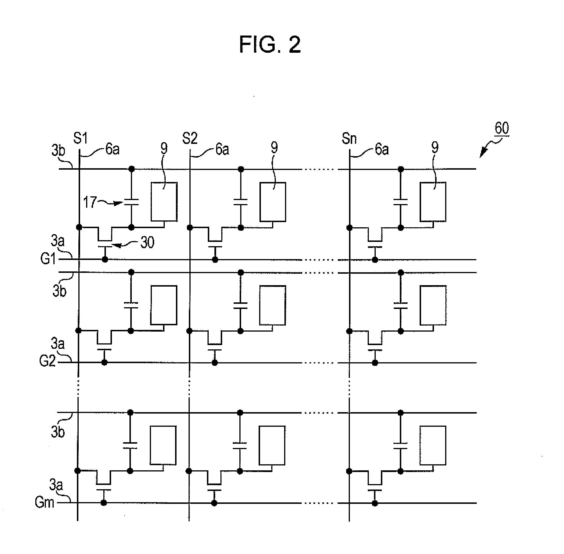
[0035] A liquid crystal device according to a first embodiment of the invention will now be described with reference to FIGS. 1 to 6. In this embodiment, a description will be made of an example of an active matrix transmissive liquid crystal panel in which thin film transistors (hereinafter referred to as TFTs) are used as switching elements. In the drawings used for the description below, the reduction scales of each layer and each component are different, so that each layer and each component have a size that can be recognized in the drawings.

Overall Structure

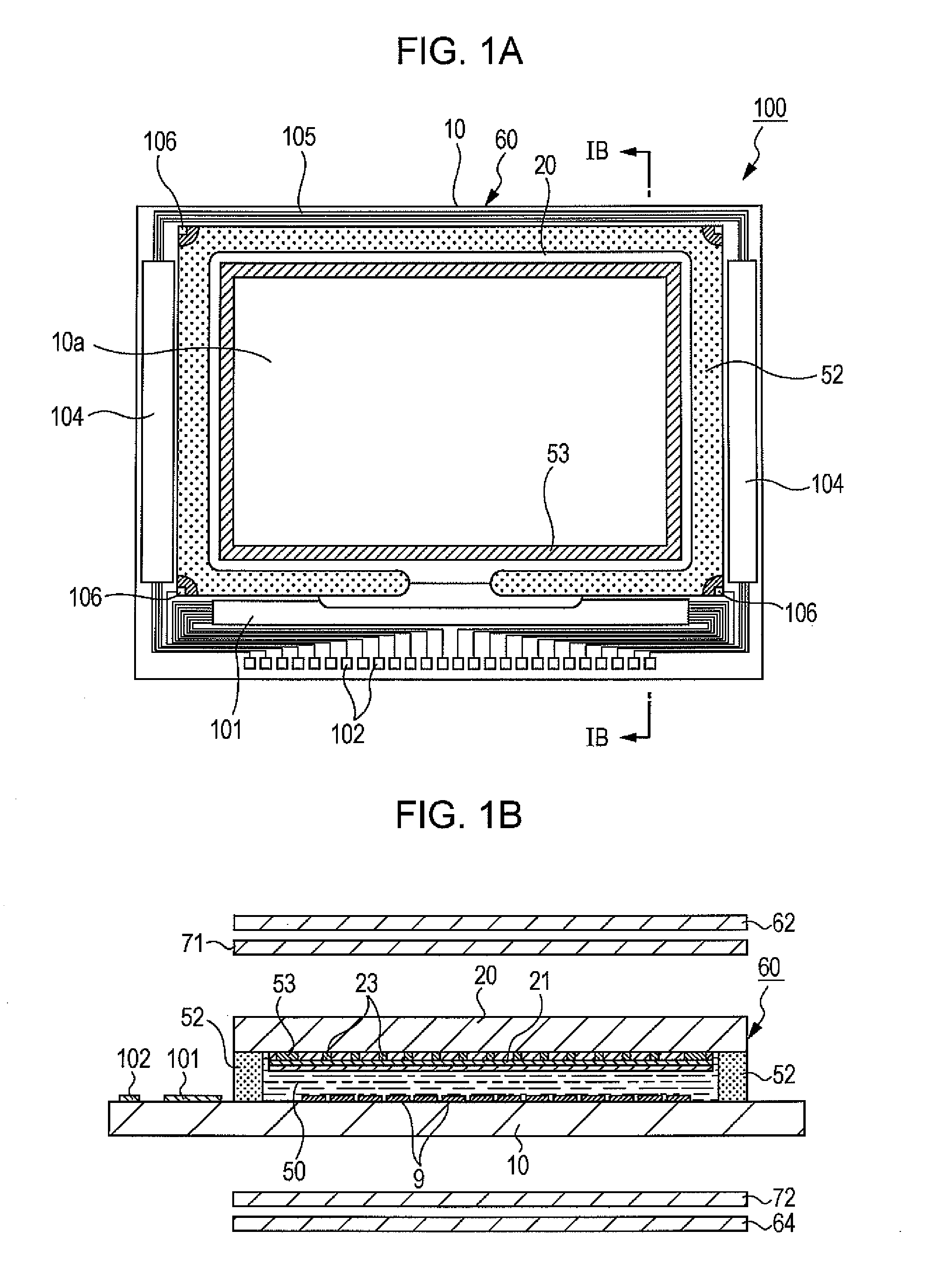
[0036]FIG. 1A is a plan view of a liquid crystal device of this embodiment, viewed from the side of a counter substrate together with constituent elements, and FIG. 1B is a cross-sectional view taken along line IB-IB in FIG. 1A. As shown in FIGS. 1A and 1B, a liquid crystal device 100 of this embodiment includes a liquid crystal panel 60, optical compensators 71 and 72 disposed so as to sandwich the liquid crystal panel 6...

second embodiment

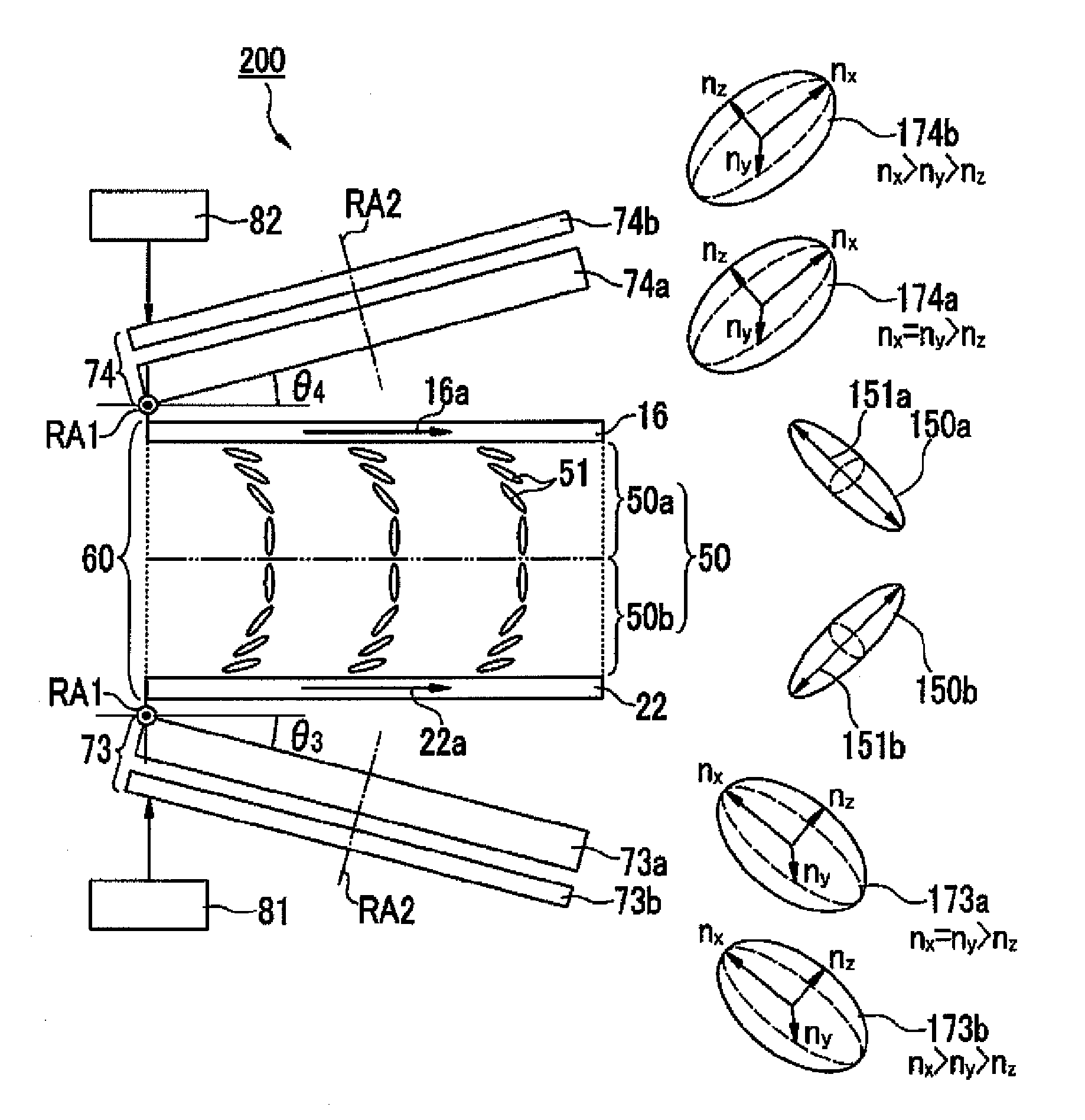
[0063] A liquid crystal device 200 of a second embodiment of the invention will now be described with reference to FIGS. 10 to 13. FIG. 10 is a view showing the schematic cross-sectional structure of the liquid crystal device 200 of this embodiment and corresponds to FIG. 6 in the first embodiment. In FIG. 10, the same constituent elements as those in the first embodiment are assigned the same reference numerals, and the description of those elements is omitted.

[0064] As shown in FIG. 10, the liquid crystal device 200 includes an optical compensator 73 disposed at the side of the back face (light-incident side) of a liquid crystal panel 60 and an optical compensator 74 disposed at the side of the front face (light-emitting side) of a liquid crystal panel 60. The optical compensator 73 is prepared by laminating two optical compensation films 73a and 73b. In this embodiment, the optical compensation film 73a is a negative C-plate (a uniaxial optical anisotropic medium that has negati...

third embodiment

[0075] A third embodiment of the invention will now be described with reference to FIG. 14. FIG. 14 is a perspective view showing the schematic structure of a liquid crystal device 300 of this embodiment. In FIG. 14, the same constituent elements as those in the above embodiments are assigned the same reference numerals, and the description of those elements is omitted.

[0076] As shown in FIG. 14, the liquid crystal device 300 includes a liquid crystal panel 60 and two optical compensators 75 and 76 disposed so as to sandwich the liquid crystal panel 60. In this embodiment, the optical compensators 75 and 76 include an optical anisotropic layer composed of a discotic compound having negative refractive index anisotropy. Their index ellipsoids 175 and 176 are schematically shown on the right side of the optical compensators 75 and 76, respectively, in the figure.

[0077] The optical compensators 75 and 76 of this embodiment include an optical anisotropic substance composed of a discot...


PUM


Abstract

A liquid crystal device includes an OCB mode liquid crystal panel including a pair of substrates and a liquid crystal layer disposed therebetween, an optical compensator provided on at least one side of the liquid crystal panel, and an optical-axis-adjusting unit that moves the optical compensator relative to the liquid crystal panel to adjust an angle formed by an optical axis of the optical compensator and an optical axis of the liquid crystal panel.

Description

BACKGROUND [0001] 1. Technical Field [0002] The present invention relates to a liquid crystal device and a projection display device. [0003] 2. Related Art [0004] In a liquid crystal projector (projection display device), illuminating light is modulated by a liquid crystal device provided as a light valve, and the modulated light is projected onto a screen to display an image. In such a projector including a liquid crystal device as a light valve, when image light includes light passing through a liquid crystal layer in an oblique direction, the black level is increased to decrease the contrast. In order to solve this problem, for example, JP-A-2002-217427 and JP-A-2002-14345 propose a technique in which an optical compensation element used in a direct-viewing-type liquid crystal display device is combined with a light valve. [0005] Recently, in order to improve the image quality of moving images, optically compensated bend (OCB) mode liquid crystal devices whose response time is sh...

Claims


Application Information

Patent Timeline
IPC IPC(8): G02F1/1335
CPCG02F1/133632G02F1/133634G02F1/1395G02F2413/105
Inventor HARUYAMA, AKIHIDENISHIMURA, JOJI
Owner JAPAN DISPLAY WEST
Why Eureka
Try Eureka