Electroless plating apparatus and electroless plating method

Inactive Publication Date: 2007-06-14
TOKYO ELECTRON LTD
View PDF1 Cites 9 Cited by
  • Summary
  • Abstract
  • Description
  • Claims
  • Application Information

AI Technical Summary

Benefits of technology

[0009] Accordingly, it is an object of the invention to provide an electroless plating apparatus and an electroless plating method which perform electroless plating on a wiring portion on a su

Problems solved by technology

This increases current-based migration of Cu atoms, so-called electromigration, which may lead to disconnection of wires, lowering the reliability.
This lowers the operational speed of the semiconductor device.
In this c

Method used


Image

  • Electroless plating apparatus and electroless plating method
  • Electroless plating apparatus and electroless plating method
  • Electroless plating apparatus and electroless plating method

Examples


Example

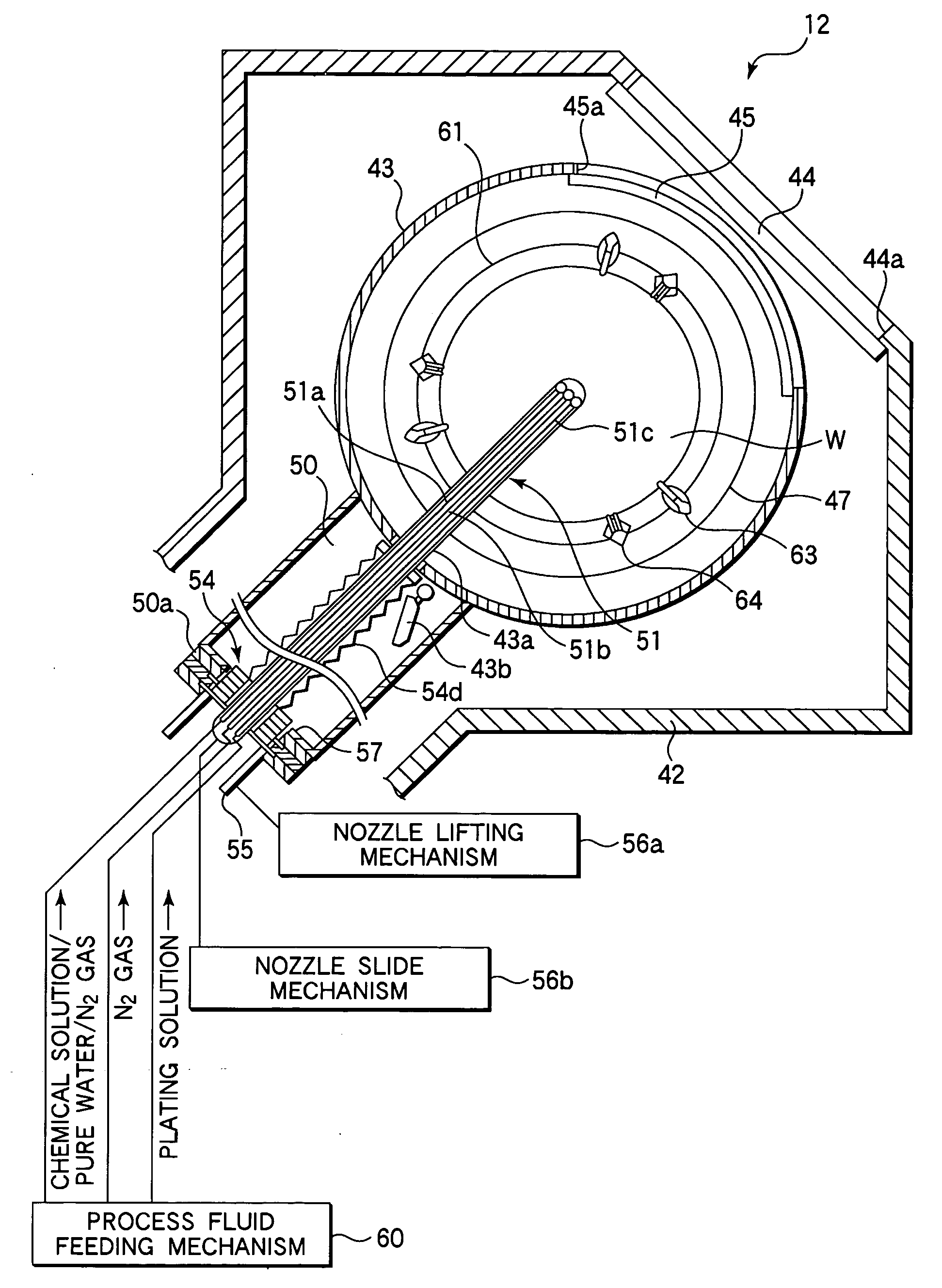
[0028] One embodiment of the present invention will be described below referring to the accompanying drawings.

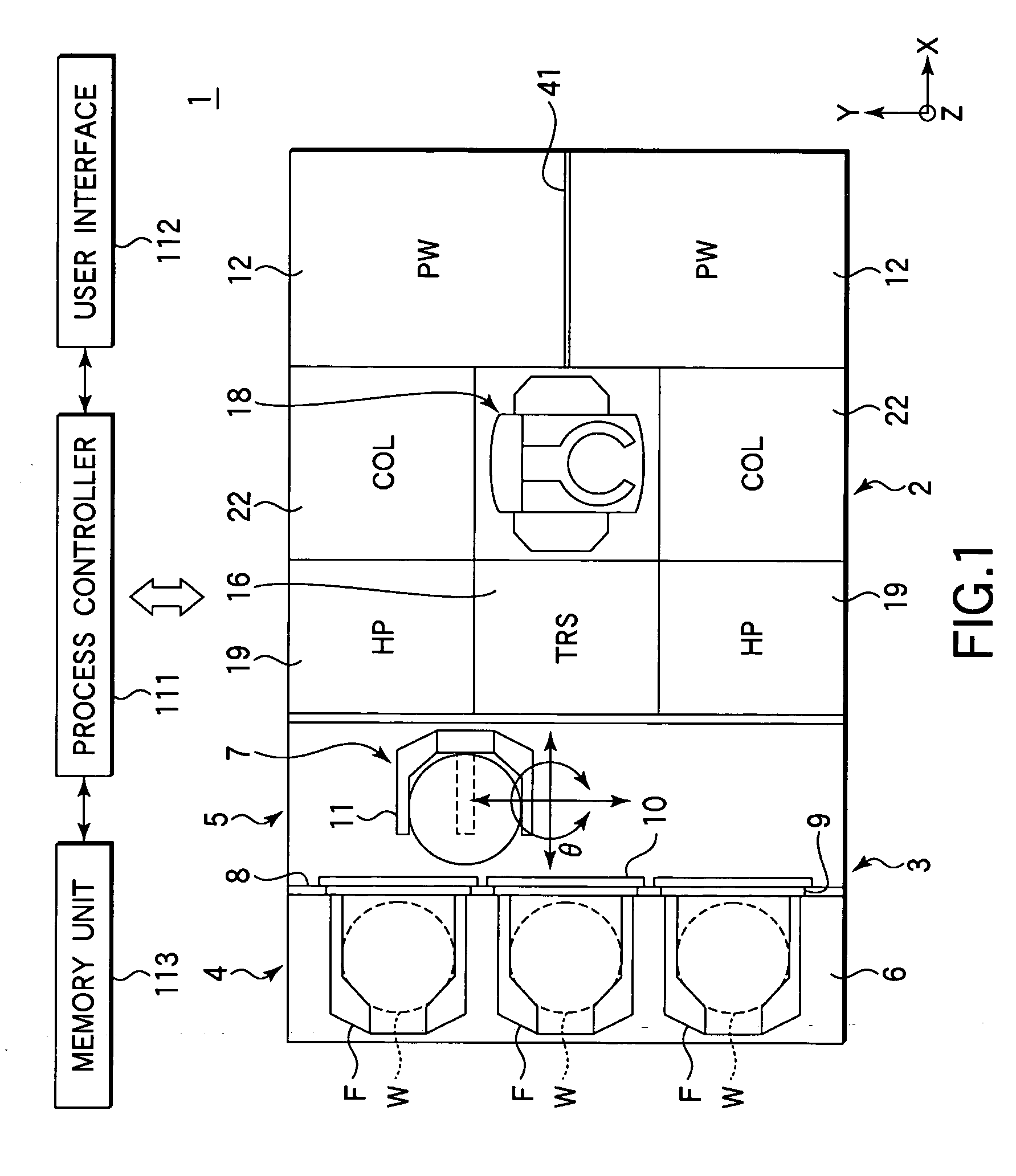
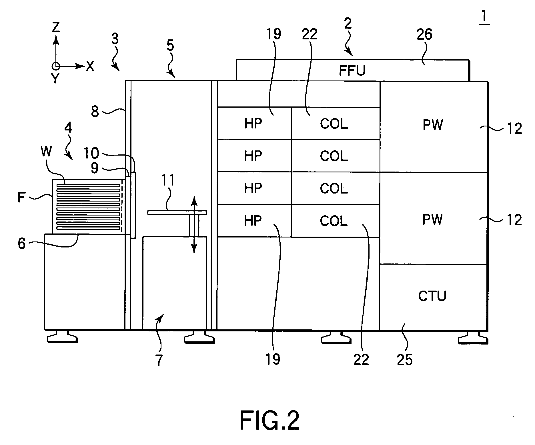
[0029]FIG. 1 is a plan view showing the schematic configuration of an electroless plating system equipped with an electroless plating unit according to one embodiment of the invention, FIG. 2 is a side view of the electroless plating system, and FIG. 3 is a cross-sectional view thereof.

[0030] An electroless plating system 1 has a processing unit 2 and a transfer in / out unit 3. The processing unit 2 performs an electroless plating process on a semiconductor wafer as a substrate to be processed, which is formed of a conductive material like silicon, (hereinafter, simply called “wafer”), and a heat treatment of the wafer before and after the electroless plating process. The transfer in / out unit 3 transfers a wafer W into and out from the processing unit 2. A wafer W in use has on its top surface a wiring portion (not shown) formed of a metal like copper (Cu). The processing u...


PUM

PropertyMeasurementUnit
Poweraaaaaaaaaa
Electrical conductoraaaaaaaaaa
Reduction potentialaaaaaaaaaa

Abstract

An electroless plating apparatus performs electroless plating on a wiring portion with a plating solution using a reducer having low reduction power. The electroless plating apparatus includes a support member with a conductive portion, which supports a substrate; a plating-solution feeding mechanism which feeds the plating solution to a top surface of the substrate supported by the support member; a metal member which is provided at the support member in such a way as to be contactable to the plating solution and dissolves into the plating solution when in contact therewith to thereby generate electrons; and an electron supply passage which supplies the electrons generated by the dissolved metal member to the wiring portion on the substrate via the conductive portion of the support member.

Description

BACKGROUND OF THE INVENTION [0001] 1. Field of the Invention [0002] The present invention relates to an electroless plating apparatus and an electroless plating method which perform electroless plating on a wiring portion formed on a substrate like a semiconductor wafer with a plating solution using a reducer having low reduction power. [0003] 2. Description of the Related Art [0004] The use of Cu (copper) for wires to be formed on a semiconductor wafer as a substrate is becoming popular in the fabrication process for semiconductor devices in order to improve the operational speed thereof. The formation of Cu wires on a substrate is generally carried out by a damascene process which forms vias and trenches to bury wires in an insulating film and bury Cu wires in the vias and trenches. [0005] Semiconductor devices having such Cu wires are having ever-finer microfabrication patterns and ever-higher integration resulting in an increased current density. This increases current-based mig...

Claims


Application Information

Patent Timeline
IPC IPC(8): B05D5/12B05D1/18B05C5/00
CPCC23C18/1619C23C18/1628H01L21/6715H01L21/6723H01L21/68728C23C18/1601
Inventor HARA, KENICHITOSHIMA, TAKAYUKIIWASHITA, MITSUAKIORII, TAKEHIKO
Owner TOKYO ELECTRON LTD
Why Eureka
Try Eureka