Treating method for probes positioned on a test card
- Summary
- Abstract
- Description
- Claims
- Application Information
AI Technical Summary
Benefits of technology
Problems solved by technology
Method used
Image

Examples
first embodiment
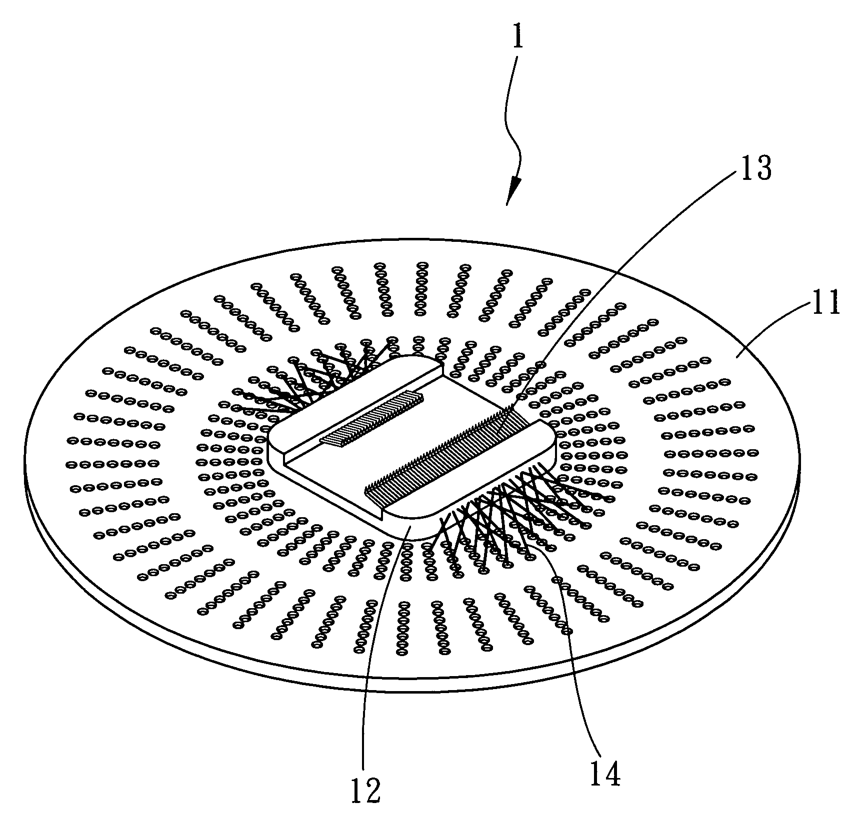
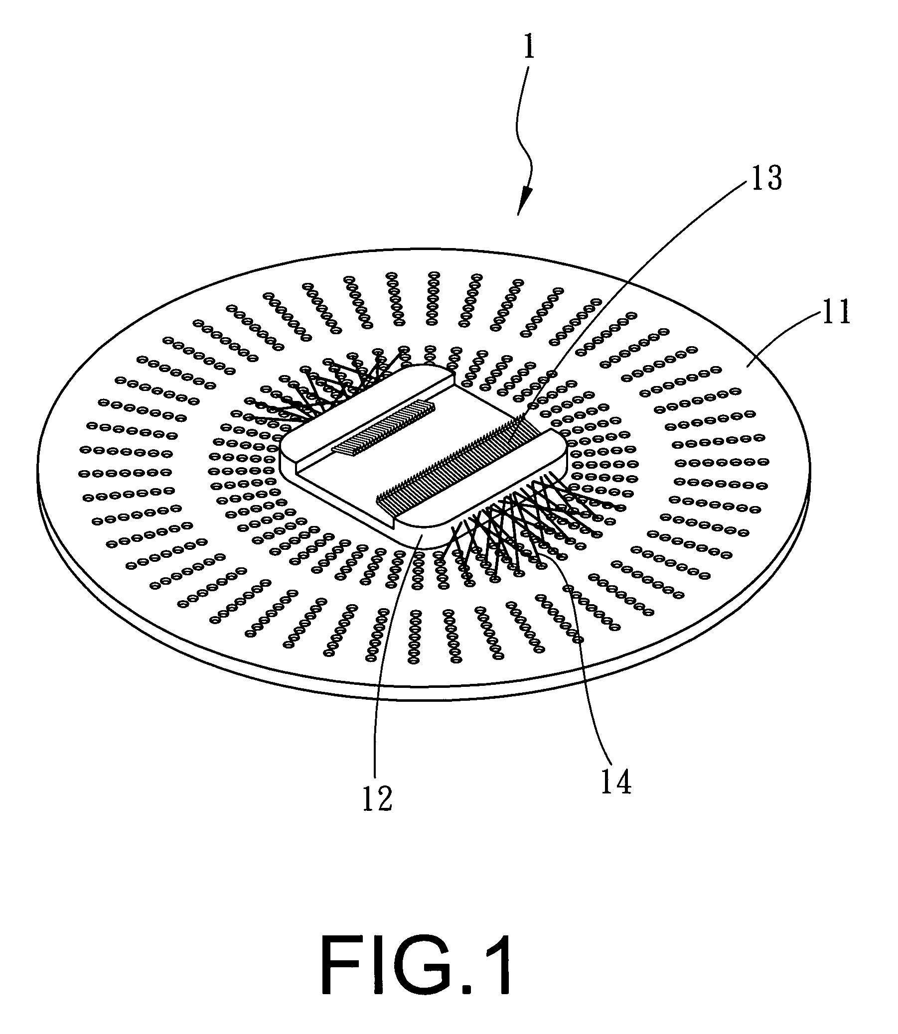
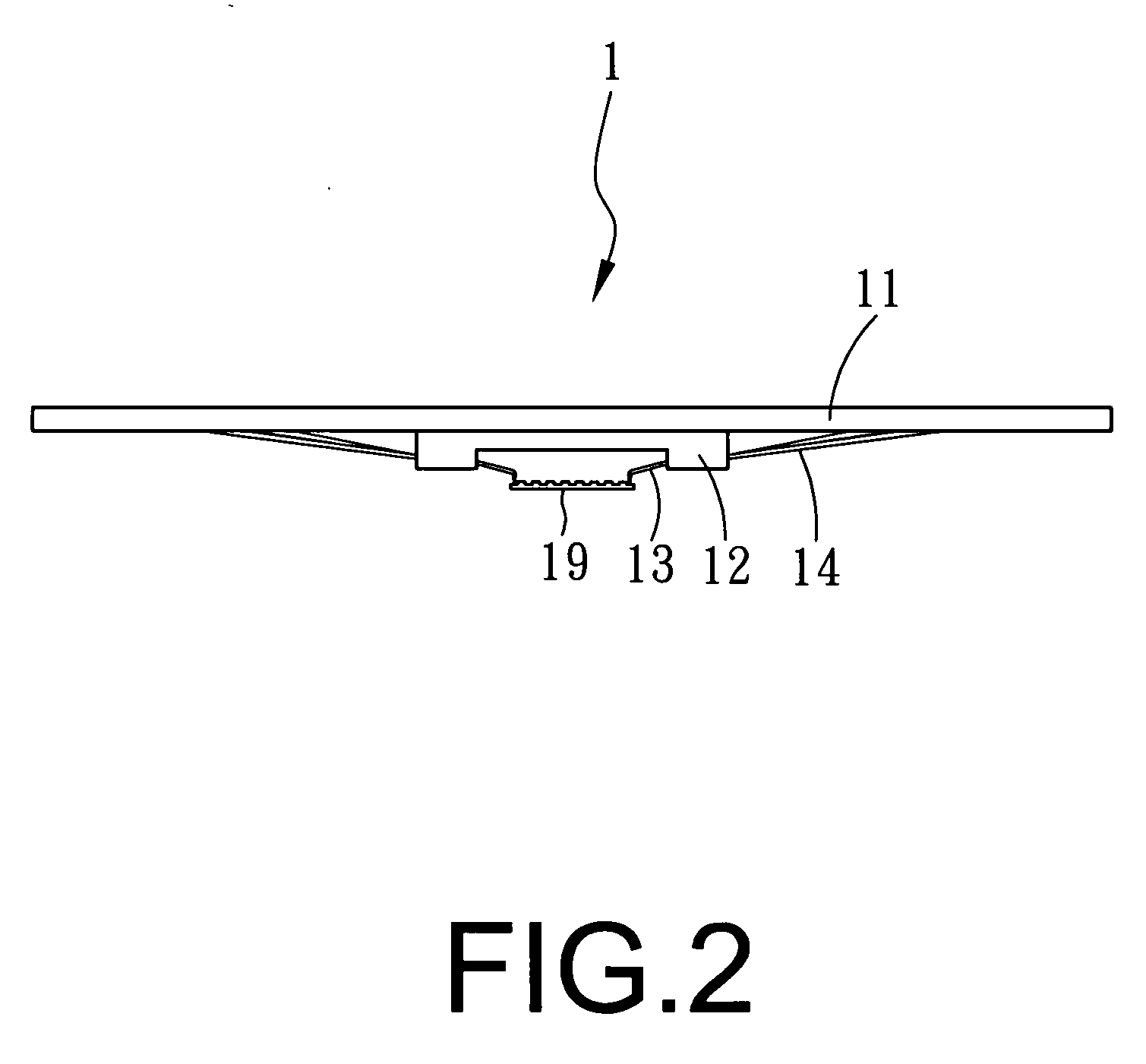
[0029] a treating method for probes positioned on a test card in the present invention, as shown in FIG. 4, includes six steps.
[0030] Probes 2 positioned on a test card are made of tungsten or tungsten alloy having rigidity and electric conductivity, as shown in FIG. 5A.
[0031] The first step is to cover the test card and the surfaces of shanks 22 of the probes 2, only exposing tips 21 of the probes 2.
[0032] The second step is to place the test card and the probes 2 in a plating device, and the plating device is vacuum plating cell.
[0033] The third step is to plate a conductive layer of film 3 on the surfaces of the uncovered tips 21 of the probes 2 for protection, as shown in FIG. 5B.
[0034] The fourth step is to repair or grind even the surfaces of the probes 2 being worn after the probes 2 are used, by removing the dirt and residue 31 on the surface of the film 3 and grinding or repairing, as shown in FIGS. 5C and 5D.
[0035] The fifth step is to cover the test card and the shan...
second embodiment
[0037] Next, a treating method for probes positioned on a test card in the present invention, as shown in FIG. 6, includes four steps, applied to the probes on the test card used and worn down, as shown in FIG. 5C.
[0038] The first step is to repair or grind even the surfaces of the probes 2; first clean dirt and residue 31 remained on the surface of the layer of film 3, and then grind or repair it smooth, as shown n FIG. 5D.
[0039] The second step is to cover the test card and portions of the probes 2 not to be plated, only exposing the surfaces of portions of the probes 2 to be plated.
[0040] The third step is to place the test card and the probes 2 in a plating device, and the plating device is a vacuum electric plating cell.
[0041] The fourth step is to plate a conductive layer of film 32 on the surfaces of the uncovered portions of the probes 2 for protection, as shown in FIG. 5E.
[0042] The materials of the layers of film 3 and 32 are not the same according to the objects or th...
third embodiment
[0045] Next, a treating method for probes positioned on a test card in the present invention, as shown in FIGS. 7 and 8, is designed for preventing electric interference between the probes 2 and short circuit caused by exterior matters falling on the probes 2, including six steps to be described below.
[0046] The first step is to cover the shanks 22 of the probes 2, only exposing the tips 21 of the probes 2.
[0047] The second step is to place the probes 2 in a plating cell, and the plating device is a vacuum plating cell.
[0048] The third step is to plate a conductive layer of film 3 on the uncovered tips 21 of the probes 2.
[0049] The fourth step is to cover the plated tips 21 of the probes 2 and let the shanks 22 of the probes 22 exposed out.
[0050] The fifth step is to place the probes 2 in a plating device again.
[0051] The sixth step is to plate an insulating and nonconductive layer of film 4 on the uncovered surfaces of the shanks 22 of the probes 2 for insulating protection.
[...
PUM
 Abstract
Description
Claims
Application Information