External electrode forming method

Active Publication Date: 2007-06-21
TDK CORPARATION
View PDF3 Cites 0 Cited by
  • Summary
  • Abstract
  • Description
  • Claims
  • Application Information

AI Technical Summary

Benefits of technology

[0012] This makes adhesion of the conductive paste particularly good in the region where the liquid is not evaporated, and thus a sufficient thickness of the third electrode portion can be secured more appropriately. Since the peripheral region of the precoat portion is easy to dry, the peripheral region first dried functions to prevent the third electrode portion from flowing off and spreading in a wet state out of the precoat portion, because of the difference of wettability.
[0013] Preferably, the third formation step is carried out prior to the first formation step and the second formation step. The external electrode can b

Problems solved by technology

However, it is difficult to freely control the viscosity of the conductive paste and it is thus difficult to control the lengths of the external electrodes from the ridgeline on each side face of the chip by adjustment of the viscosity of the conductive paste.
From this investigation, the Inventors found that an increase in the amount of the conductive paste increased the length of an extension of the external electrode on the side face of the chip in the direction away from the ridgeline and along the side face, but also inevitably increased the width of an extension in the direction along the ridge

Method used


Image

  • External electrode forming method
  • External electrode forming method
  • External electrode forming method

Examples


Example

[0025] The expertise of the invention can be readily understood in view of the following detailed description with reference to the accompanying drawings presented by way of illustration only. Subsequently, an embodiment of the present invention will be described with reference to the accompanying drawings. The same portions will be denoted by the same reference symbols as much as possible, without redundant description.

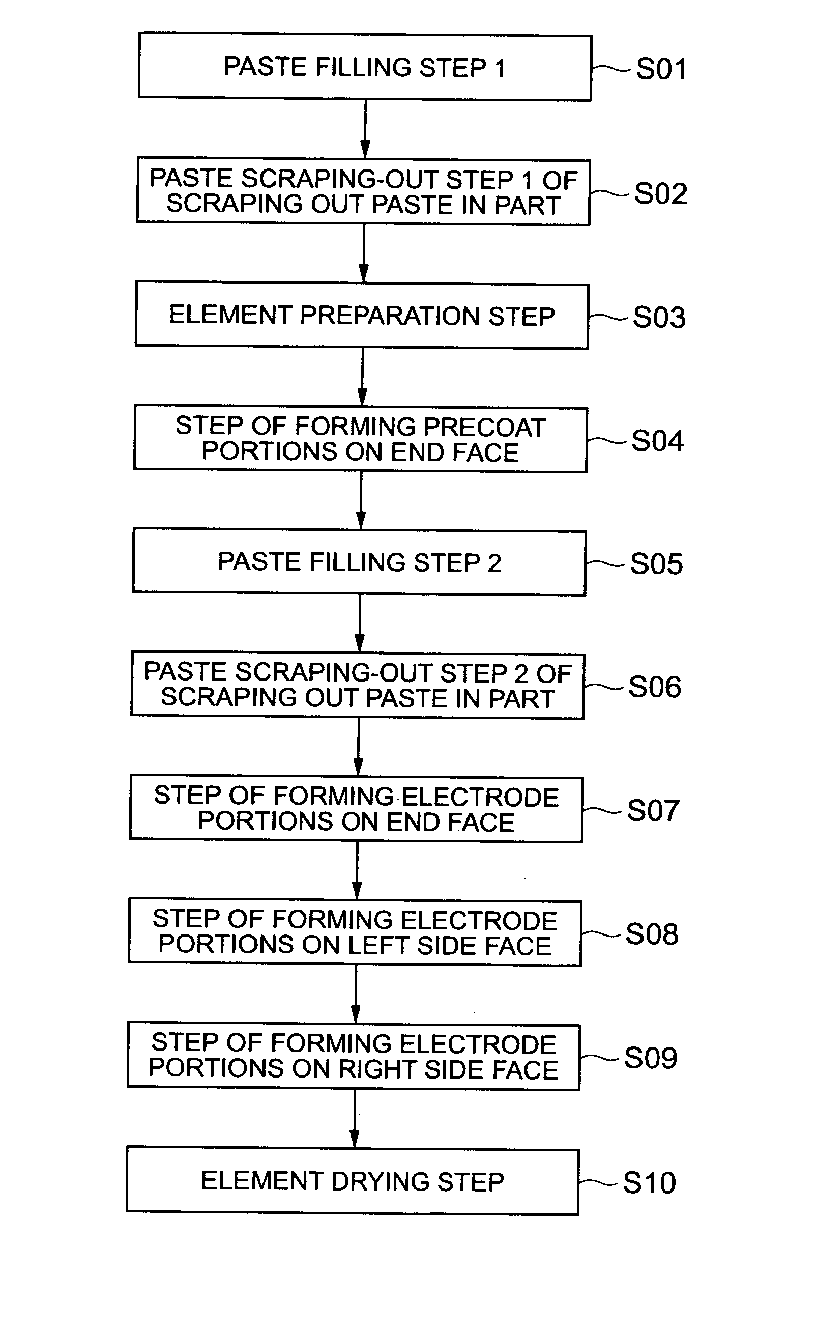
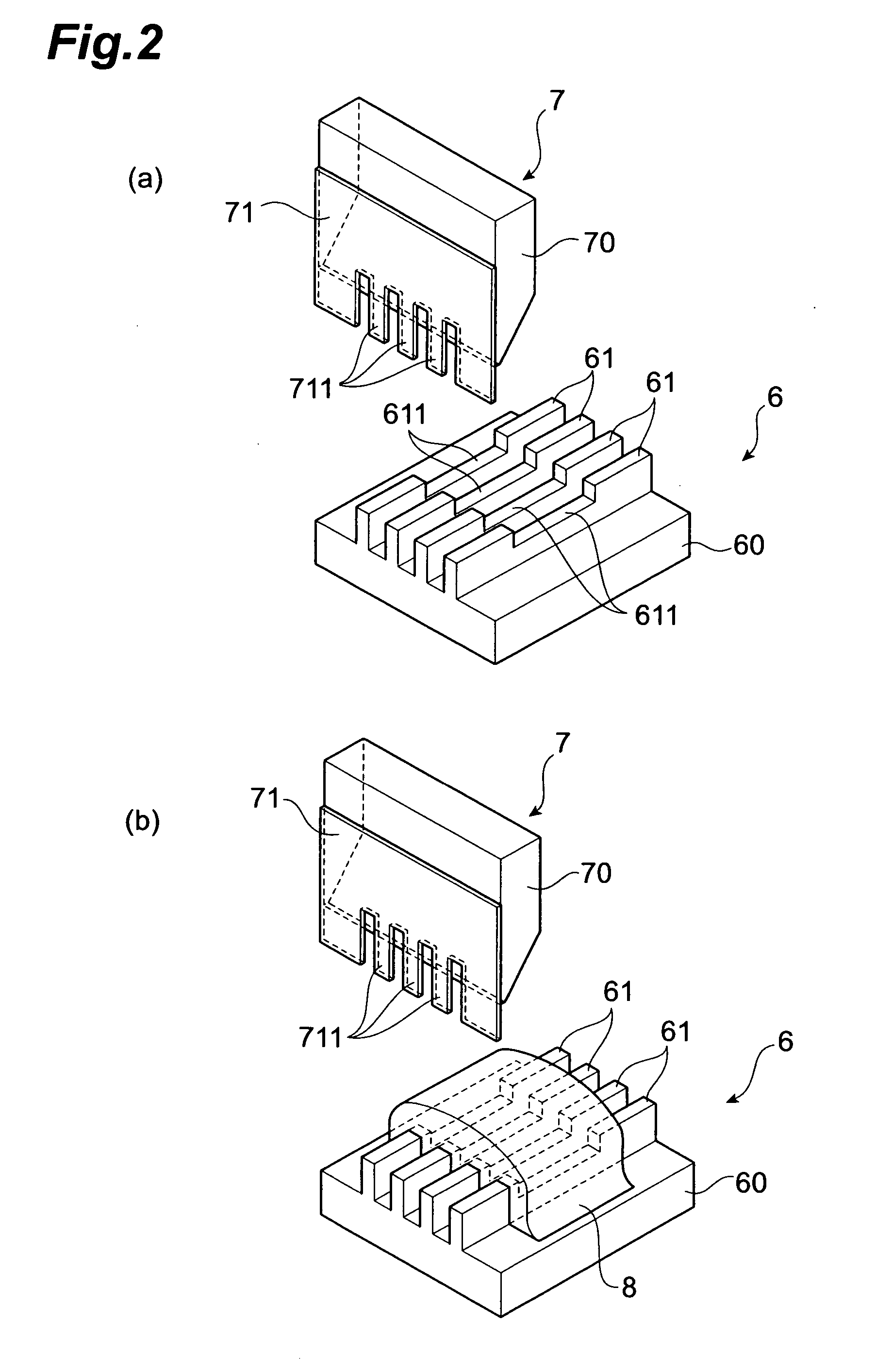
[0026] An external electrode forming method, which is an embodiment of the present inventions will be described. The external electrode forming method of the present embodiment is outlined as follows. First, an application bed (jig) with grooves is prepared, and a conductive paste is attached along wall faces and bottom faces of the grooves. Thereafter, a chip (element) is put into the grooves and moved vertically and horizontally to form external electrodes on an end face (third face) and on two side faces (first face and second face) of the chip. Subsequently, the...


PUM

PropertyMeasurementUnit
Electrical conductoraaaaaaaaaa

Abstract

An element forming an electronic component has a first face and a second face facing each other, and a third face adjacent to each of the first face and the second face. A method of forming an external electrode of the electronic component involves a pre-formation step, first to third formation steps, and an electrode formation step. The pre-formation step is to apply a conductive paste onto the third face and to evaporate at least a part of a liquid contained in the applied conductive paste, to form a precoat portion expected to become a part of a third electrode portion. The first formation step is to apply the conductive paste from a direction opposite to the first face, onto the first face to form a first electrode portion. The second formation step is to apply the conductive paste from a direction opposite to the second face, onto the second face to form a second electrode portion. The third formation step is to apply the conductive paste onto the third face so as to cover the precoat portion, to form the third electrode portion. The electrode formation step is to dry the element to form the external electrode consisting of the first electrode portion, the second electrode portion, and the third electrode portion. The first electrode portion, the second electrode portion, and the third electrode portion are formed so as to connect with each other.

Description

BACKGROUND OF THE INVENTION [0001] 1. Field of the Invention [0002] The present invention relates to a method of forming an external electrode of an electronic component. [0003] 2. Related Background Art [0004] One of methods of forming an external electrode of an electronic component is the method described in U.S. Pat. No. 5,753,299. This method is to form external electrodes on an end face of a chip being an element to become an electronic component, and on side faces adjacent to the end face. More specifically, consecutively projecting portions called fingers of a comb-shaped plate are arranged at positions opposite to the end face of the chip, and a conductive paste for formation of external electrodes is applied onto tips of the fingers. Subsequently, the fingers are brought into contact with the chip and are slid in directions perpendicular to the extending direction of the chip to rub the conductive paste onto the chip, thereby forming external electrodes. SUMMARY OF THE INV...

Claims


Application Information

Patent Timeline
IPC IPC(8): H01B13/00H01C17/28H01G13/00
CPCH01G13/006H01L21/4867H01L23/49805H01L24/11H01L2224/13099H01L2924/01002Y10T29/43H01L2924/01033H01L2924/01082H05K3/403H01L2924/01005H01L2924/01006H01L2224/1131H01L2924/01015B05D5/12H05K3/32
Inventor ONODERA, KOKURIMOTO, SATOSHITOZAWA, YOJIOOTSUKI, SHIROU
Owner TDK CORPARATION
Why Eureka
Try Eureka