Dual metal gate self-aligned integration

a metal gate and self-aligning technology, applied in the field of semiconductor structure, can solve the problems of further degradation of device performance, using a polysilicon gate,

Inactive Publication Date: 2007-06-21
GLOBALFOUNDRIES US INC
View PDF5 Cites 71 Cited by
  • Summary
  • Abstract
  • Description
  • Claims
  • Application Information

AI Technical Summary

Benefits of technology

[0006] A semiconductor structure including at least one n-type field effect transistor (nFET) and at least one p-type field effect transistor (pFET) that both include a metal gate, without including an upper polysilicon gate electrode is provided. More particularly, the present in

Problems solved by technology

However, there are also some problems associated with using a polysilicon gate.
Another problem with polysilicon gates is that the dopant in the polysilicon gate, such as boron, can easily diffuse through the thin gate dielectric causing further degradation of the device performance.
Another pro

Method used


Image

  • Dual metal gate self-aligned integration
  • Dual metal gate self-aligned integration
  • Dual metal gate self-aligned integration

Examples


Embodiment Construction

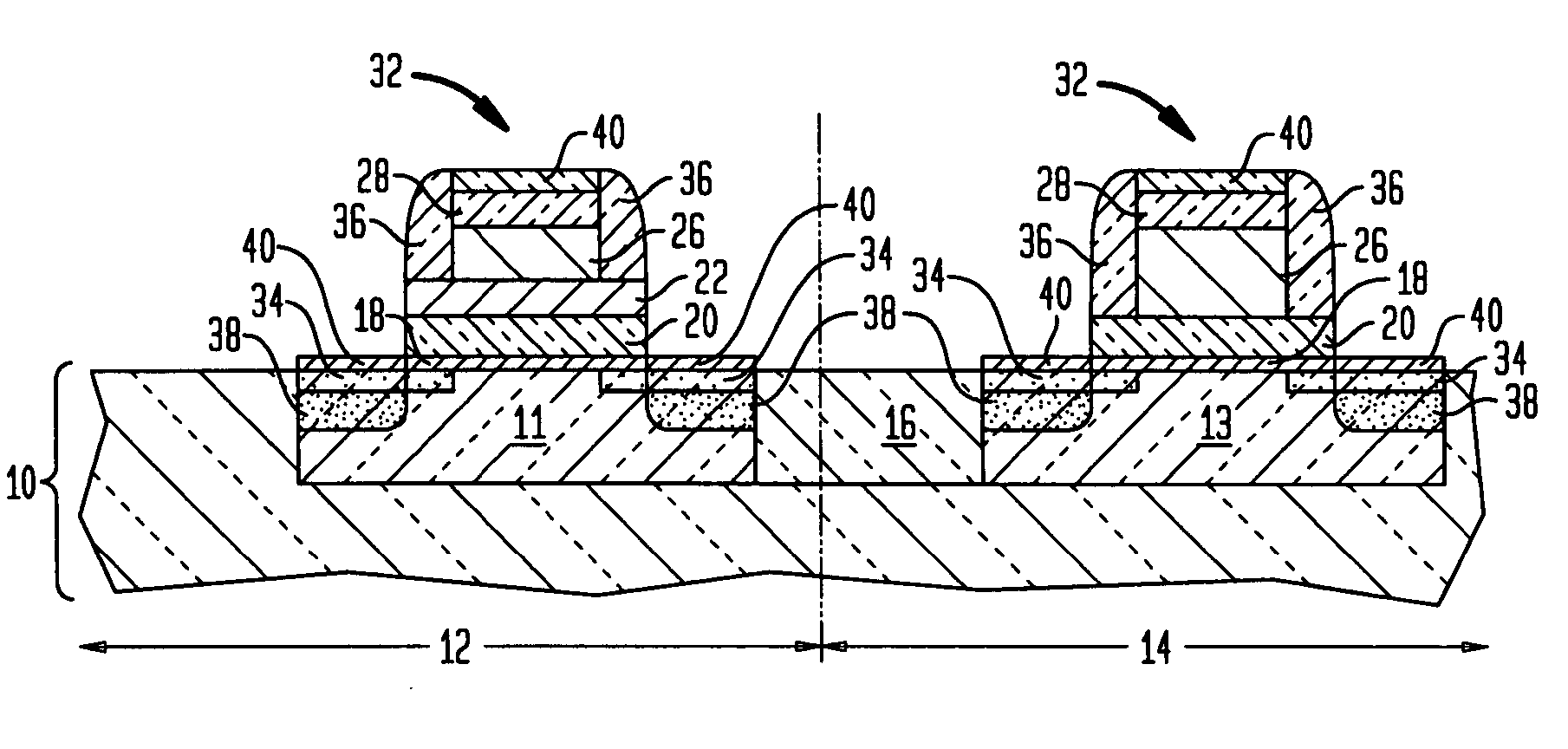
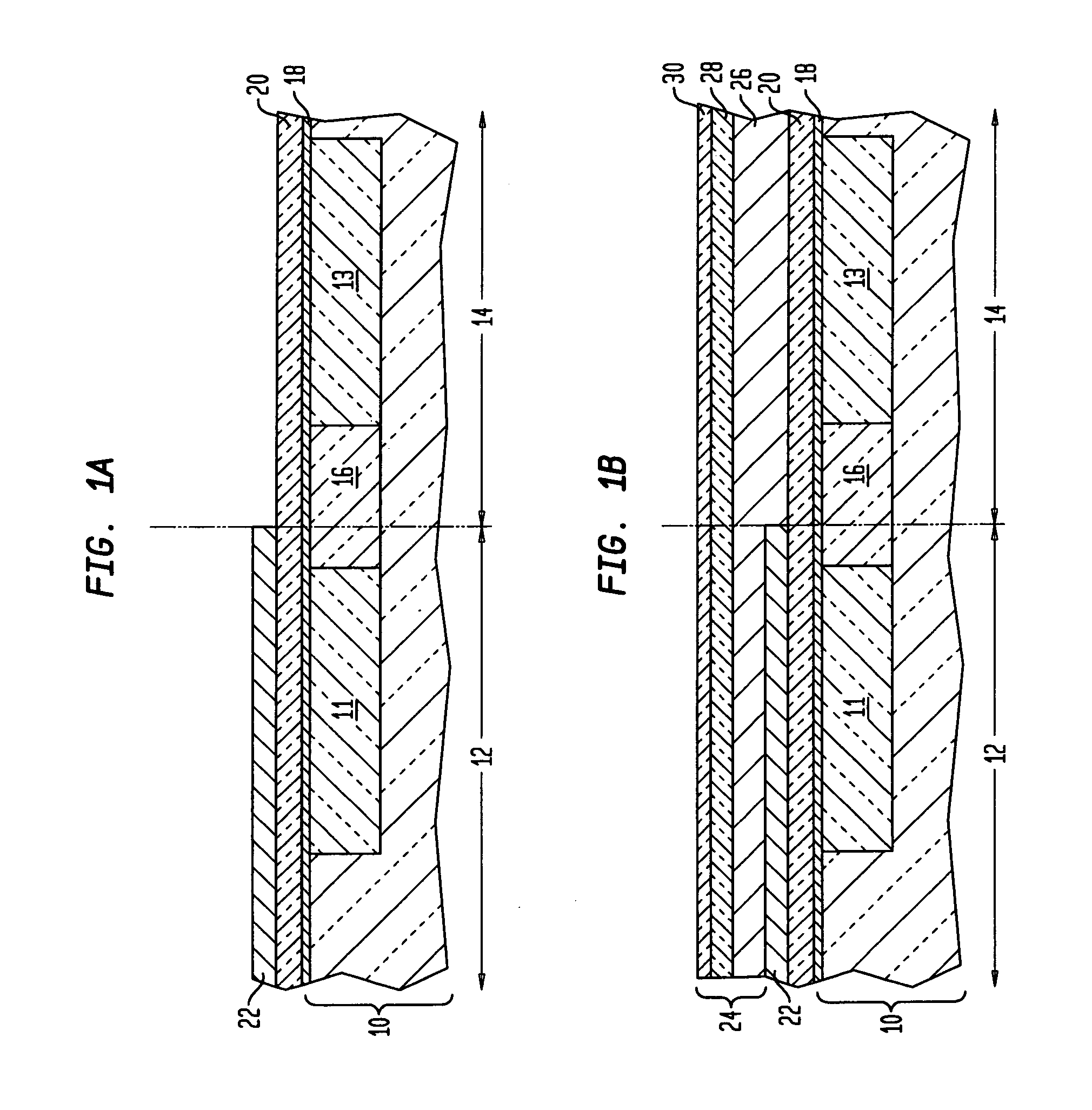
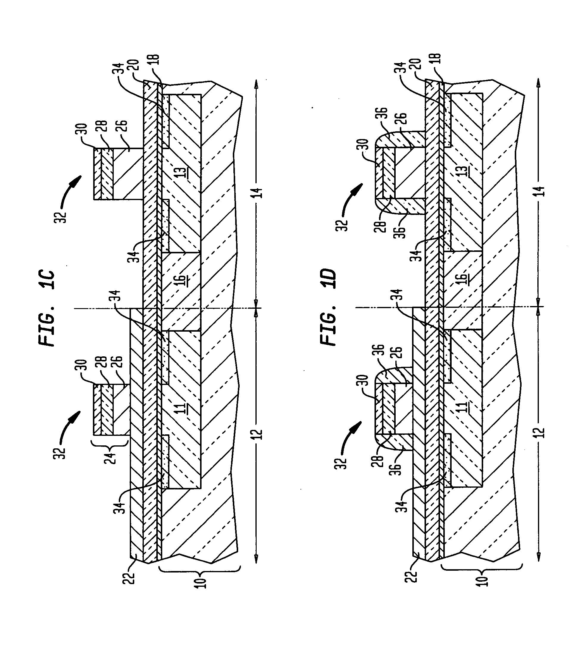
[0019] The present invention, which provides a semiconductor structure and a method of fabricating the same, will now be described in greater detail by referring to the drawings that accompany the present application. It is noted that the drawings of the present application are provided for illustrative purposes and, as such, they are not drawn to scale. It is also noted that in the drawings, like and / or corresponding elements are referred to by like reference numerals.

[0020] It is further observed that the drawings of the present application show a fragment of a semiconductor substrate including a single nFET device region and a single pFET device region. Although such an embodiment is specifically shown and described, the present invention is not limited to a single region for the pFET devices and the nFET devices, but instead contemplates a plurality of each of such device regions located throughout the remaining portions of the substrate. Also, more that one nFET device and pFE...


PUM


Abstract

A semiconductor structure including at least one n-type field effect transistor (nFET) and at least one p-type field effect transistor (pFET) that both include a metal gate having nFET behavior and pFET behavior, respectively, without including an upper polysilicon gate electrode is provided. The present invention also provides a method of fabricating such a semiconductor structure.

Description

FIELD OF THE INVENTION [0001] The present invention relates to a semiconductor structure, and more particularly to a semiconductor structure including at least one n-type field effect transistor (nFET) and at least one p-type field effect transistor (pFET) that both include a metal gate, without including an upper polysilicon gate electrode. The present invention also provides a method of fabricating such a semiconductor structure. BACKGROUND OF THE INVENTION [0002] In standard complementary metal oxide semiconductor (CMOS) devices, polysilicon is typically the standard gate material. The technology of fabricating CMOS devices using polysilicon gates has been in a constant state of development, and is now widely used in the semiconductor industry. One advantage of using polysilicon gates is that they can sustain high temperatures. However, there are also some problems associated with using a polysilicon gate. For example, due to the poly-depletion effect and relative high electrical...

Claims


Application Information

Patent Timeline
IPC IPC(8): H01L29/78H01L21/8238
CPCH01L21/823842
Inventor CALLEGARI, ALESSANDRO C.CHUDZIK, MICHAEL P.DORIS, BRUCE B.NARAYANAN, VIJAYPARUCHURI, VAMSI K.STEEN, MICHELLE L.
Owner GLOBALFOUNDRIES US INC
Why Eureka
Try Eureka