Semiconductor device, and inspection method thereof

a semiconductor and semiconductor technology, applied in semiconductor/solid-state device testing/measurement, basic electric elements, instruments, etc., can solve the problems of deterioration in yield, the connection terminal used for stacking cannot be subjected to inspection, so as to facilitate electrical continuity inspection and improve the reliability of stacking-type semiconductor modules

Active Publication Date: 2007-06-21
PANASONIC CORP
View PDF3 Cites 18 Cited by
  • Summary
  • Abstract
  • Description
  • Claims
  • Application Information

AI Technical Summary

Benefits of technology

[0016]A semiconductor device and an inspection method thereof according to the present invention are devised in order to solve the aforementioned problems. An object of the present invention is to facilitate an inspection of electrical continuity between a connection terminal provided for a connection with a semiconductor device to be stacked on a semiconductor device and a bump electrode provided for a connection with an external apparatus, and to improve reliability of a stacking-type semiconductor module.
[0023]The semiconductor device according to the present invention further comprises an annular wire formed of a wire on an uppermost layer of the substrate and connected to any one of the connection terminals in the respective pairs, thereby to suppress voltage fluctuations.
[0027]According to the present invention, it is possible to facilitate an inspection of electrical continuity between a connection terminal provided for a connection with a semiconductor device to be stacked on a semiconductor device and a bump electrode provided for a connection with an external apparatus, and to improve reliability of a stacking-type semiconductor module.

Problems solved by technology

This leads to deterioration in yield.
Consequently, a package in which a chip is mounted on a sub-substrate cannot be subjected to an inspection.
However, a connection terminal used for stacking cannot be subjected to an inspection.
However, if this technique is applied to a stacking-type semiconductor module, a contact pad to be used as a stacking connection terminal is damaged due to contact with a probe.
Consequently, connection failure readily occurs.
In this method, however, a contact pad is damaged as described above, so that connection failure readily occurs.
Further, a tester to be used herein is expensive.

Method used


Image

  • Semiconductor device, and inspection method thereof
  • Semiconductor device, and inspection method thereof
  • Semiconductor device, and inspection method thereof

Examples


first embodiment

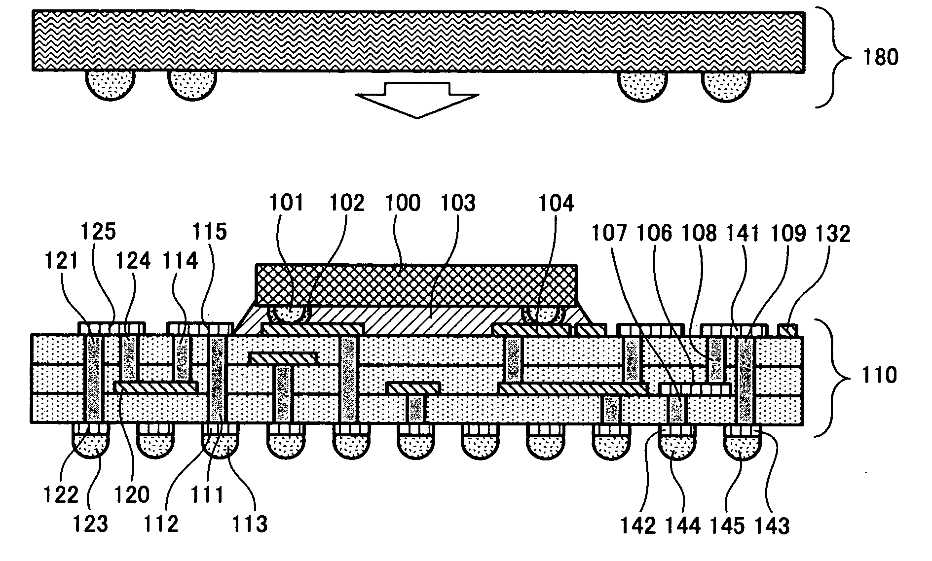
[0043]With reference to FIGS. 1 and 2, description will be given of a semiconductor integrated circuit in a first embodiment of the present invention.

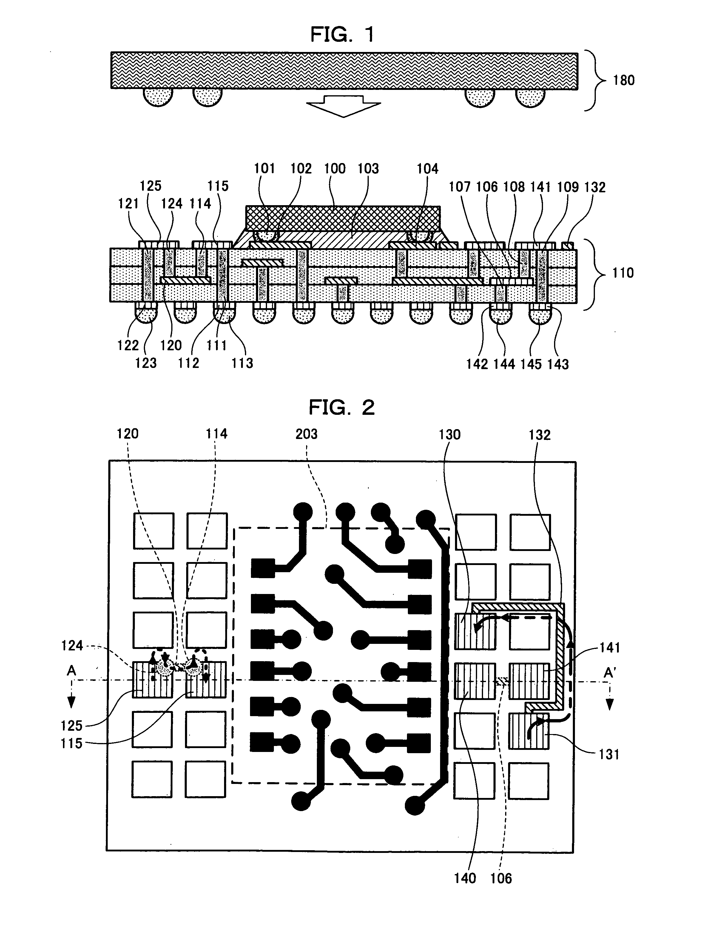
[0044]FIG. 1 is a sectional view taken along a line A-A′ in FIG. 2 and illustrates a configuration of a stacking-type semiconductor device in the first embodiment of the present invention. FIG. 2 briefly illustrates a configuration of a substrate in the first embodiment of the present invention when being seen from above.

[0045]In FIG. 1, a semiconductor device 180 is stacked on a substrate 110 having a semiconductor chip 100 mounted thereon. A bump electrode 101 connects between the semiconductor chip 100 and the substrate 110. The bump electrode 101 is bonded to the substrate 110 through a conductive adhesive 102. A space between the semiconductor chip 100 and the substrate 110 is filled with an underfill resin 103. In the first embodiment and subsequent embodiments, the semiconductor chip 100 is mounted on the substrate 110 in a typi...

second embodiment

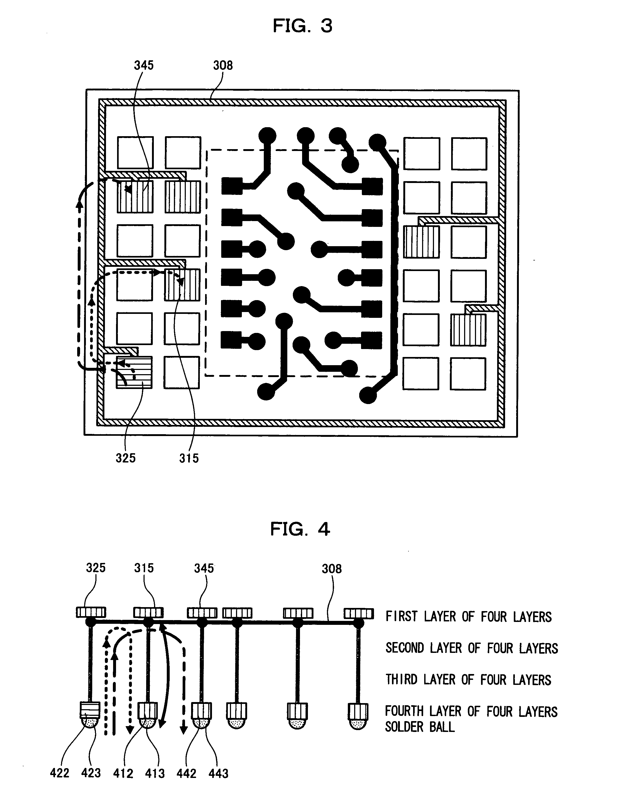
[0057]With reference to FIGS. 3 and 4, description will be given of a semiconductor integrated circuit in a second embodiment of the present invention. In this embodiment, description will be given of a connection among the plurality of connection terminals described in the first embodiment in order to perform an inspection.

[0058]FIG. 3 briefly illustrates a configuration of a substrate in the second embodiment of the present invention when being seen from above. FIG. 4 schematically illustrates a configuration of a connection in the second embodiment of the present invention. Herein, specific description is given with reference to FIG. 4.

[0059]In FIG. 3, connection terminals 315, 325 and 345 are provided for a connection with a semiconductor device to be stacked, respectively. A wire 308 connects among the connection terminals 315, 325 and 345, and is formed on an outer periphery of a first layer (a top face) of the substrate so as to surround the substrate.

[0060]In FIG. 4, the con...

third embodiment

[0066]With reference to FIGS. 5 to 7, description will be given of a semiconductor integrated circuit in a third embodiment of the present invention. In this embodiment, description will be given of a connection among connection terminals in a case that the wire formed on the first layer of the substrate described in the second embodiment cannot connect among the connection terminals.

[0067]FIG. 5 briefly illustrates a configuration of a substrate in the third embodiment of the present invention when being seen from above. FIG. 6 is a sectional view taken along a line A-A′ in FIG. 5 and illustrates the configuration of the substrate in the third embodiment of the present invention. FIG. 7 schematically illustrates a configuration of a connection in the third embodiment of the present invention. Herein, specific description is given with reference to FIG. 7.

[0068]In FIG. 5, connection terminals 515, 525 and 345 are provided for a connection with a semiconductor device to be stacked, r...


PUM


Abstract

In a substrate for a stacking-type semiconductor device including a connection terminal provided for a connection with a semiconductor chip to be stacked and an external terminal connected to the connection terminal through a conductor provided in a substrate, connection terminals of a power supply, a ground and the like, which terminals have an identical node, are electrically continuous with each other. Thus, it is possible to facilitate an inspection of electrical continuity between each connection terminal and an external terminal corresponding to each connection terminal by minimum addition of inspecting terminals. Further, it is possible to improve reliability of a stacking-type semiconductor module.

Description

BACKGROUND OF THE INVENTION[0001](1) Field of the Invention[0002]The present invention relates to a semiconductor device having another semiconductor device stacked thereon, and an inspection method of the semiconductor device.[0003](2) Description of the Related Art[0004]In response to demand for small-sized, high-performance electronic apparatuses such as portable telephones and digital cameras, there is developed a stacking-type semiconductor module including electronic components, in particular, semiconductor chips integrated with each other in a stacked manner (refer to JP2004-363126A).[0005]For example, a second semiconductor package containing a second semiconductor chip is stacked on a first semiconductor package containing a first semiconductor chip.[0006]Such a stacking-type semiconductor module is subjected to an inspection after the aforementioned stacking process. Herein, a stacking-type semiconductor module evaluated as a defective is discarded. Alternatively, in the s...

Claims


Application Information

Patent Timeline
Patent Type & Authority Applications(United States)
IPC IPC(8): H01L23/12
CPCG01R31/2853H01L2224/2919H01L22/34H01L24/83H01L24/85H01L25/0657H01L2224/16225H01L2224/73204H01L2224/83102H01L2224/83851H01L2224/92125H01L2924/14H01L2924/15192H01L2924/15311H01L2224/85H01L2224/32225G01R31/318513H01L2924/00014H01L2924/00H01L2224/48H01L2224/45015H01L2924/207H01L2224/45099
Inventor SHINAGAWA, MASATOSHIKAWABATA, TAKESHI
Owner PANASONIC CORP
Why Eureka
Try Eureka