Unified memory and controller

a controller and memory technology, applied in the field of memory devices, can solve the problems of inability to provide automatic address mapping, and the device suffers from two shortcomings

Inactive Publication Date: 2007-06-28
GREENLIANT
View PDF67 Cites 58 Cited by
  • Summary
  • Abstract
  • Description
  • Claims
  • Application Information

AI Technical Summary

Problems solved by technology

However, it is believed the OneNAND device suffers from two shortcomings.
A second problem is believed to be a shortcoming of the OneNAND device is that it cannot provide for automatic address mapping.
However, it is believed that the controller portion of the DiskOnChip device does not have any on board nonvolatile bootable memory, such as NOR memory.

Method used


Image

  • Unified memory and controller
  • Unified memory and controller
  • Unified memory and controller

Examples


first embodiment

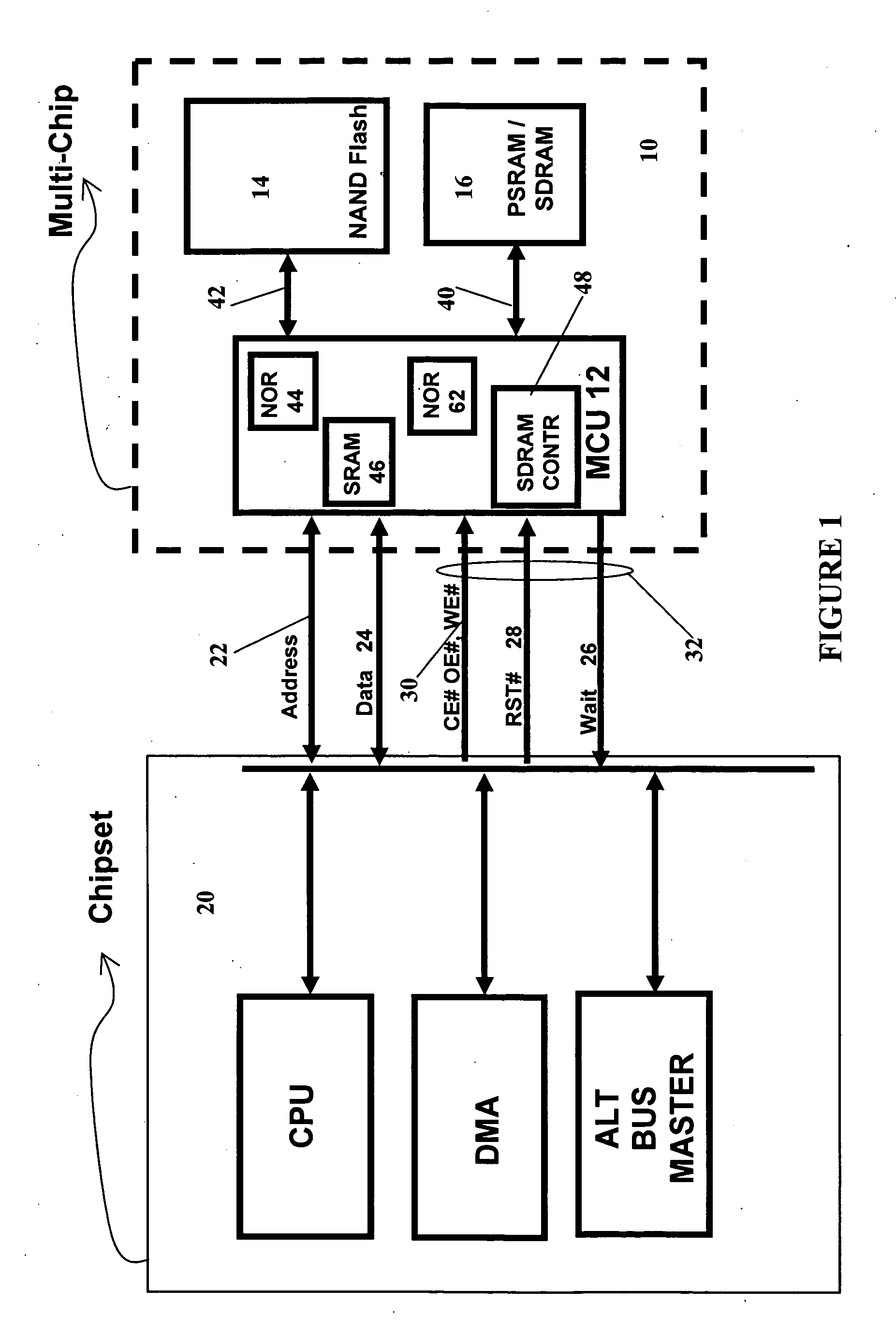
[0022] Referring to FIG. 1, there is shown a memory device 10. The memory device 10 comprises a memory controller 12, a NAND memory 14, and a RAM memory 16. The memory device 10 interfaces with a host device 20, through a first RAM address bus 22, a first RAM data bus 24, and a plurality of control signals such as wait 26, RST# 28, and CE#, OE#, and WE# 30, all of which are well known to one skilled in the art of control signals for a RAM bus. Hereinafter unless otherwise specified, all of the control signals on the wait 26, RST# 28 and CE#, OE# and WE# 30 are referred to as first RAM control bus 32. The first RAM address bus 22, the first RAM data bus 24 and the first RAM control bus 32 are connected from the host device 20 to the memory controller 12 of the memory device 10. Further, as discussed previously, the interface between the memory device 10 and the host device 20 can be via a serial bus in which the data, address and control buses are serially connected between the host ...

second embodiment

[0076] Referring to FIG. 4 there is shown a memory device 110. The memory device 110 is similar to the memory device 10 shown in FIG. 1. Thus, like parts with like numerals will be designated. The only difference between the memory device 110 and the memory device 10 is that in the memory device 100, the second RAM bus 40 connects the RAM memory 100 directly to the host device 20, rather then to the memory controller 12. Thus, in the memory device 110, the host device has direct access and control of the RAM memory 100.

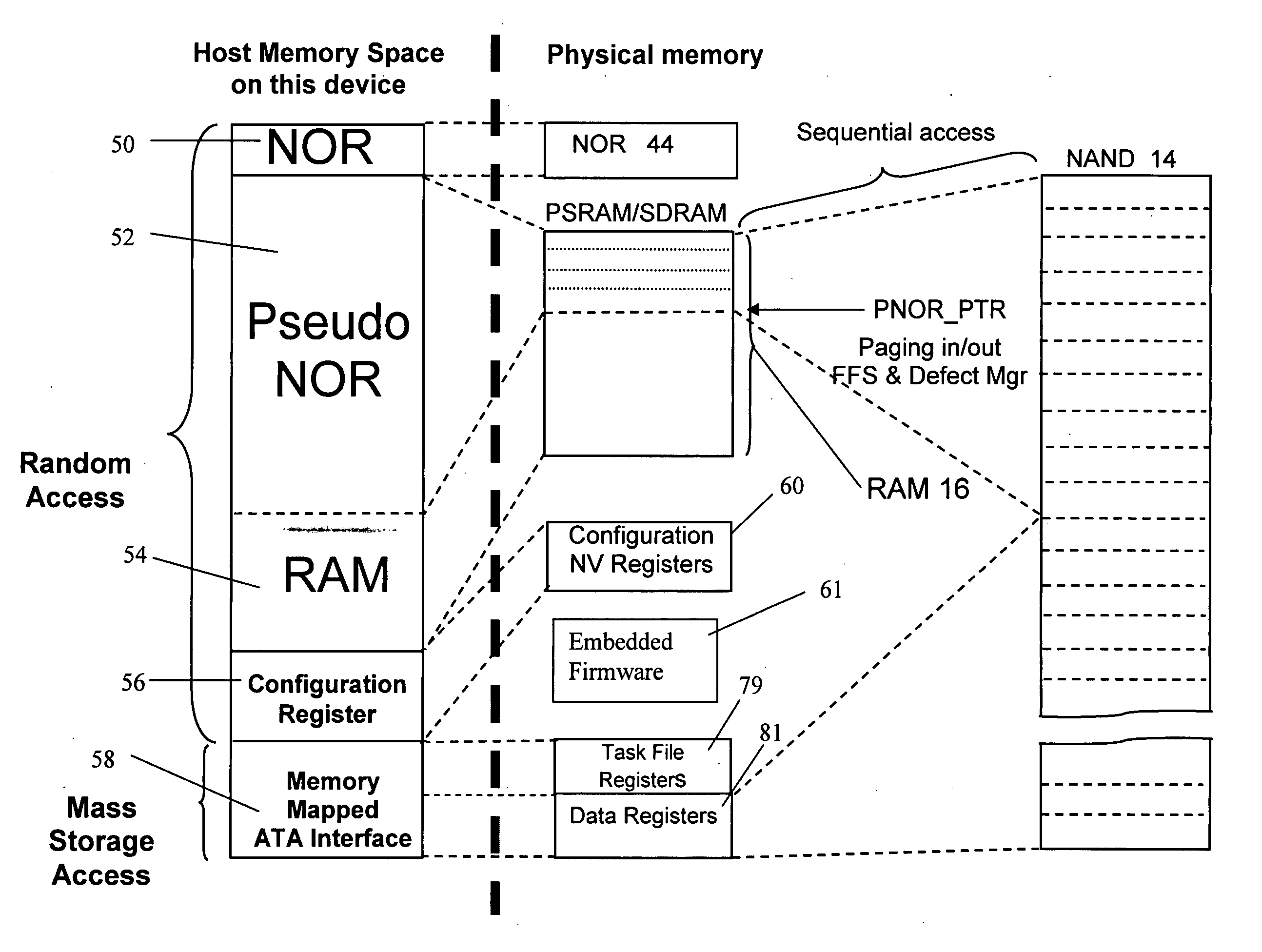
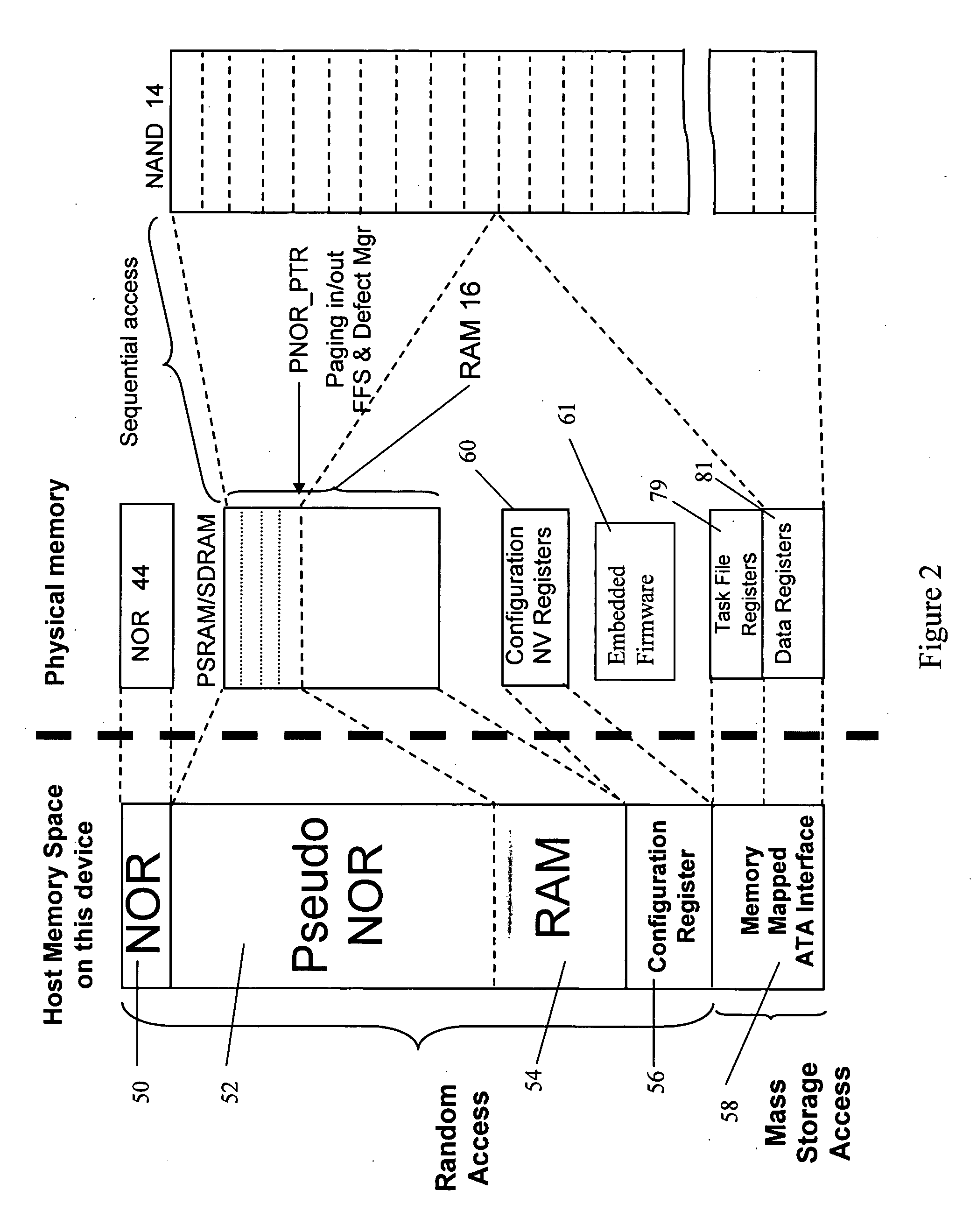
[0077] This difference between the embodiment of the memory device 10 and the embodiment of the memory device 110 is reflected in the memory mapping shown in FIG. 5. Similar to the memory device 10, the memory mapping for the memory device 110 comprises a NOR memory access portion 50 which is mapped to the NOR memory 44, a PNOR memory access portion 52 which is mapped to the RAM memory 16 in the memory device 110, which is then mapped to the NAND memory 14, and a RAM ...


PUM


Abstract

A memory device has a controller. The controller has a first address bus for receiving a RAM address signals, a first data bus for receiving RAM data signals, and a first control bus for receiving RAM control signals. The controller further has a second address bus for interfacing with a volatile RAM memory, a second data bus for interfacing with the volatile RAM memory, and a second control bus for interfacing with the volatile RAM memory. The controller further has a third address / data bus for interfacing with a non-volatile NAND memory, and a third control bus for interfacing with non-volatile NAND memory. The memory device further having a RAM memory connected to said second address bus, said second data bus, and said second control bus. The memory device further having a non-volatile NAND memory connected to the third address / data bus and to the third control bus. The controller also has a non-volatile bootable memory, and further has means to receive a first address on the first address bus and to map the first address to a second address in the non-volatile NAND memory, with the volatile RAM memory serving as cache for data to or from the second address in the non-volatile NAND memory, and means for maintaining data coherence between the data stored in the volatile RAM memory as cache and the data at the second address in the non-volatile NAND memory.

Description

[0001] This application claims the priority of a provisional application 60 / 754,937 filed on Dec. 28, 2005, whose disclosure is incorporated herein in its entirety.TECHNICAL FIELD [0002] The present invention relates to a memory device and more particularly to a memory device that has the capability of receiving address and data in conventional random address format, and map that data / address to either a NOR memory, a RAM memory, a RAM memory acting as a cache for a NAND memory thereby emulating a Pseudo-NOR (PNOR) operation, and an ATA format Non-Volatile NAND memory. The address and data are received from one or more processors either via a single bus or a plurality of buses. The present invention also relates to a memory controller with an embedded bootable NOR memory used in such a memory device. BACKGROUND OF THE INVENTION [0003] Volatile random access memory, such as SRAM or DRAM (or SDRAM) or PSRAM (hereinafter collectively referred to as RAM), are well known in the art. Typi...

Claims


Application Information

Patent Timeline
Patent Type & Authority Applications(United States)
IPC IPC(8): G11C14/00
CPCG06F13/1694G06F12/00G06F12/10G06F13/16
Inventor LIN, FONG-LONGYEH, BING
Owner GREENLIANT
Why Eureka
Try Eureka