Object and bonding method thereof

Inactive Publication Date: 2007-06-28
DELTA ELECTRONICS INC
View PDF3 Cites 2 Cited by
  • Summary
  • Abstract
  • Description
  • Claims
  • Application Information

AI Technical Summary

Benefits of technology

[0014] As mentioned above, the object and the bonding method of the invention can utilize existing equipment to form a solder ball on a pad by printing. The invention can be

Problems solved by technology

Thanks to the advances in technology and in view of the requirements for compactness and lightness in electronic products, conventional dual in-line packaged (DIP) or quad flat packaged (QFP) chips cannot satisfy modem needs.
Moreover, their electrical properties and thermal conductivity are inferior.
However, the manual bonding method outlined above has time-consumption, inh

Method used


Image

  • Object and bonding method thereof
  • Object and bonding method thereof
  • Object and bonding method thereof

Examples


Example

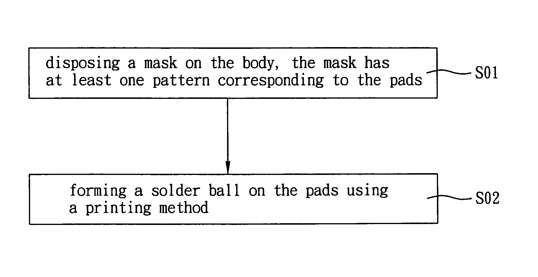
[0022] The present invention will be apparent from the following detailed description, which proceeds with reference to the accompanying drawings, wherein the same references relate to the same elements.

[0023] As shown in FIG. 4, an object 4 according to a preferred embodiment of the invention includes a body 41, at least one pad 42, and at least one solder ball 43. In this embodiment, the object 4 can be a ball grid array (BGA) package. However, the invention is not limited to this case. The object 4 can also be an electronic device, a semiconductor device, a chip, a package, a structure to be reworked, or any other object to be bonded. The body 41 has a surface 411.

[0024] The number of the pad 42 can be one, two or more than two. When the number of the pad 42 is not one, the pads 42 can be arranged on the surface 411 in an array. The material of the pads 42 can be copper, lead, aluminum, gold, silver, tin, bismuth, or their alloys.

[0025] The solder balls 43 are correspondingly ...


PUM


Abstract

A bonding method of an object having at least one pad on a surface of the object includes the steps of: putting a mask on the object, when the mask has at least one pattern corresponding to the pad; and printing to form a solder ball on the pad by a printing method.

Description

CROSS REFERENCE TO RELATED APPLICATIONS [0001] This Non-provisional application claims priority under 35 U.S.C. §119(a) on Patent Application No(s). 094145984 filed in Taiwan, Republic of China on Dec. 23, 2005, the entire contents of which are hereby incorporated by reference. BACKGROUND OF THE INVENTION [0002] 1. Field of Invention [0003] The invention relates to an object and a bonding method thereof. In particular, the invention pertains to an object with a solder ball and the bonding method thereof. [0004] 2. Related Art [0005] Thanks to the advances in technology and in view of the requirements for compactness and lightness in electronic products, conventional dual in-line packaged (DIP) or quad flat packaged (QFP) chips cannot satisfy modem needs. There is a restriction on the number of pins in the above-mentioned chips. Moreover, their electrical properties and thermal conductivity are inferior. Therefore, ball grid array (BGA) packaged chips have become the trend. The pins ...

Claims


Application Information

Patent Timeline
IPC IPC(8): H01L21/44
CPCH01L21/4853H01L24/11H01L24/12H01L24/81H01L2224/1132H01L2224/13099H01L2224/13111H01L2224/13124H01L2224/13139H01L2224/13144H01L2224/13147H01L2224/81052H01L2224/81801H01L2924/01013H01L2924/01029H01L2924/01047H01L2924/01074H01L2924/01075H01L2924/01079H01L2924/01082H05K3/1216H05K3/3484H05K2203/043H05K2203/0557H01L2924/01006H01L2924/01019H01L2924/01023H01L2924/01033H01L2924/014H01L2224/11334H01L24/05H01L2224/05568H01L2224/05573H01L2224/05611H01L2224/05624H01L2224/05639H01L2224/05644H01L2224/05647H05K3/3485H01L2924/00014
Inventor CHENG, CHI-MINGLAN, ZHENG-PING
Owner DELTA ELECTRONICS INC
Why Eureka
Try Eureka