Changeable USB memory stick

a memory stick and usb technology, applied in the field of personal storage devices, can solve the problems of increasing complexity, inability to add more ic elements and wiring layout, and inconvenient application, so as to save circuit board space, increase application inconvenience, and not increase the size of the memory stick

Inactive Publication Date: 2007-06-28
POWER DATA COMM & CHIEN YUAN CHEN
View PDF11 Cites 11 Cited by
  • Summary
  • Abstract
  • Description
  • Claims
  • Application Information

AI Technical Summary

Benefits of technology

[0011] Accordingly, only a single common bus is required for the memory stick itself, and a function of a portion of circuit junctions in the common bus is shared between the multi-memory card interface and the USB interface; therefore, it will not increase a size of memory stick and increase an inconvenience in application. Correspondingly, only a connection port corresponding to the common bus is required to be installed on the electronic device applied with the memory stick, then a data transmission with the memory stick can be performed through the USB transmission interface or the multi-memory card transmission interface, thereby achieving the objects of saving a space of circuit board, simplifying a layout and assembling of the circuit board, increasing an overall reliability, and reducing inventory and cost of logistics.

Problems solved by technology

Moreover, these two storage devices are not easily got wet or damaged like the disks, thereby allowing many consumers to replace the disks with these two storage devices for carrying.
As a transmission interface used for connecting the memory card is not the same as that used for connecting the memory stick in an electronic device like an ordinary personal computer or notebook computer; the transmission interface for the memory stick is a USB junction, whereas the transmission interface for the memory card is a conduction terminal which is called the golden finger; therefore, a circuit board should be installed with two interfaces corresponding to the USB connection port and the memory card connector respectively, which is rather inconvenient in application.
In other words, the miniaturization of digital equipment is primarily dependent upon the installation of internal IC elements and circuit board layout which will be getting more complicated as the increase of functions.
However, due to a limitation of narrowness of circuit layout, it is impossible to add more IC elements and wiring layout.
Assembling more elements will also cause a drawback that the digital equipment will be enlarged.

Method used


Image

  • Changeable USB memory stick
  • Changeable USB memory stick
  • Changeable USB memory stick

Examples


Embodiment Construction

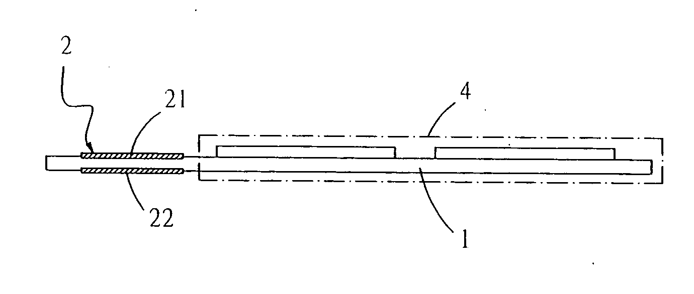
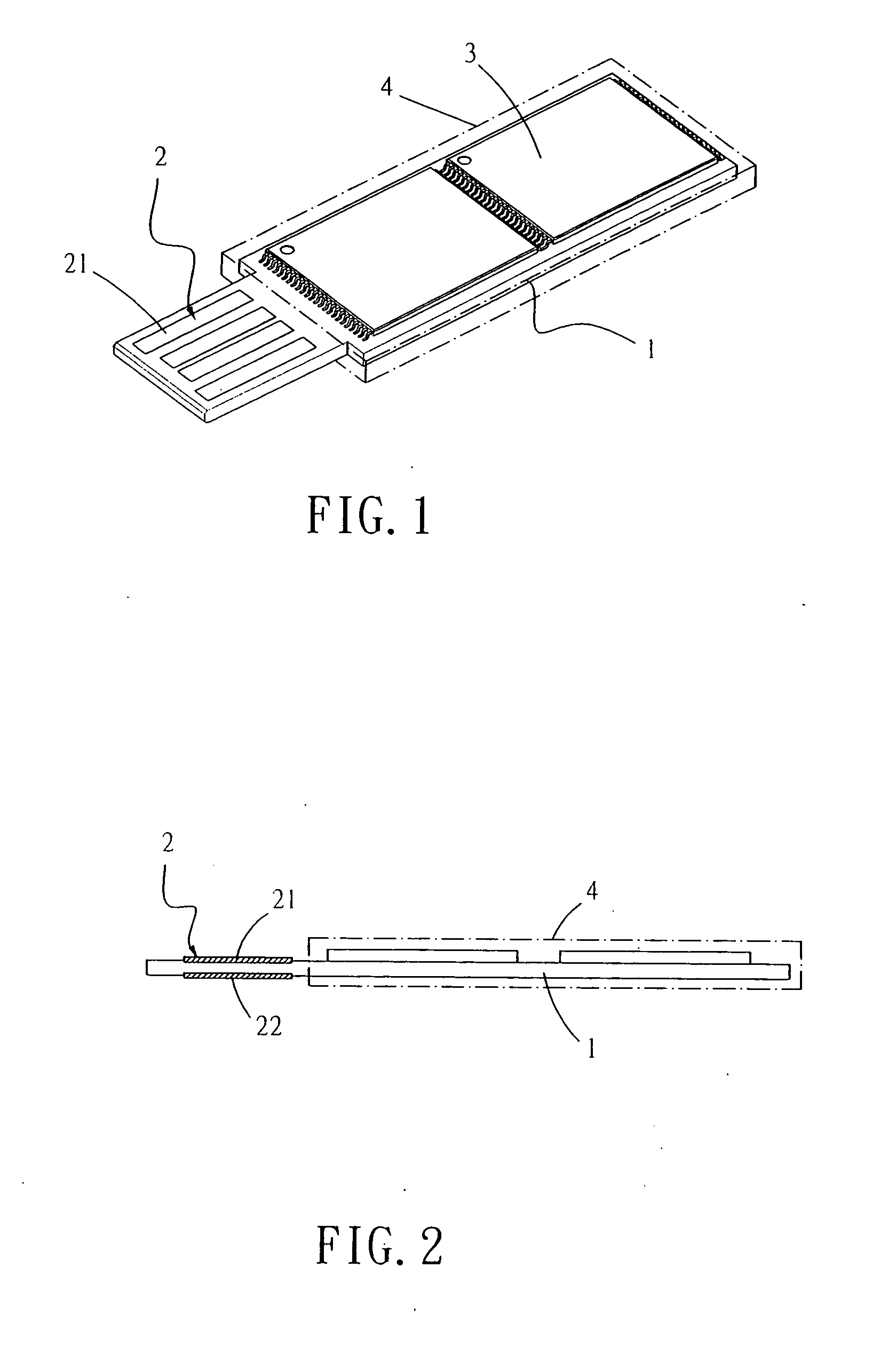
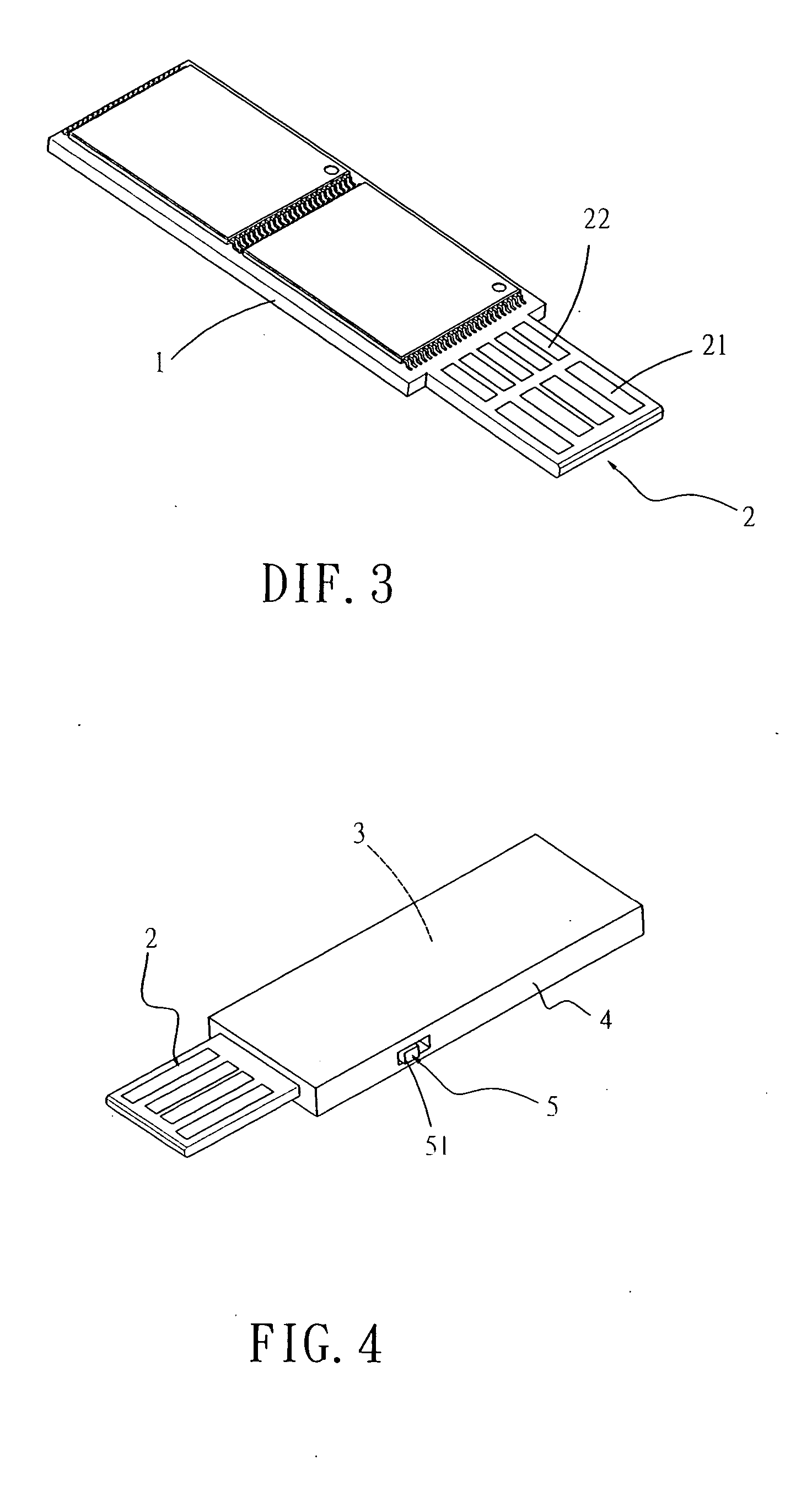
[0017] Referring to FIG. 1 and FIG. 2, it shows a structural diagram of basic components of a memory stick of the present invention. The memory stick comprises a substrate 1 which is provided with a common bus 2, a linking wiring, and IC elements including a related control chip, a switch circuit, and a memory module 3. A layer of casing 4 is wrapped on an exterior of the substrate 1 with only the common bus 2 being exposed at an end of the substrate 1, so as to constitute a necessary shielding to the IC elements on the substrate 1.

[0018] The common bus 2 is provided with a first circuit contact block 21 and at least a second circuit contact block 22, wherein the configuration of circuit junctions in the first contact block 21 is complied with the corresponding pattern of USB connection port, which is primarily used to enable the memory stick to perform a data transmission with an interconnected electronic device through the USB transmission interface; and some circuit junctions in...


PUM


Abstract

A changeable USB memory stick includes primarily a common bus which is provided with a multi-memory card interface and a USB interface. The common bus is complied with the format of a USB junction, and is provided with a transmission function of a plurality of memories. The USB memory stick can perform a signal access with a USB transmission interface or a multi-memory card transmission interface including an SD transmission interface, an MMC transmission interface, an MS PRO transmission interface, an XD transmission interface, an SM transmission interface, and a CF transmission interface of an electronic device, by interconnecting with a corresponding connection port through the single common bus.

Description

BACKGROUND OF THE INVENTION [0001] (a) Field of the Invention [0002] The present invention relates to a personal storage device and more particularly to a kind of USB (Universal Serial Bus) memory stick which can perform data access with a USB transmission interface or a multi-memory card transmission interface of an electronic device by interconnecting to a corresponding connection port through a single common bus. [0003] (b) Description of the Prior Art [0004] As the market of small size digital equipment such as a digital camera, a camcorder, an MP3 player, a mobile phone, etc., is getting more and more prosperous, its interior key elements will be directly affected. To correspond with a miniaturization and sophistication of these kinds of products, the development of technology of key elements is also toward miniaturization and chip design, and the circuit board used for configuring these mini IC (Integrated Circuit) elements is also getting smaller and smaller, while its densit...

Claims


Application Information

Patent Timeline
Patent Type & Authority Applications(United States)
IPC IPC(8): G06F13/20
CPCG06F13/387
Inventor CHEN, CHIEN-YUAN
Owner POWER DATA COMM & CHIEN YUAN CHEN
Why Eureka
Try Eureka