Nano tube cell and memory device using the same

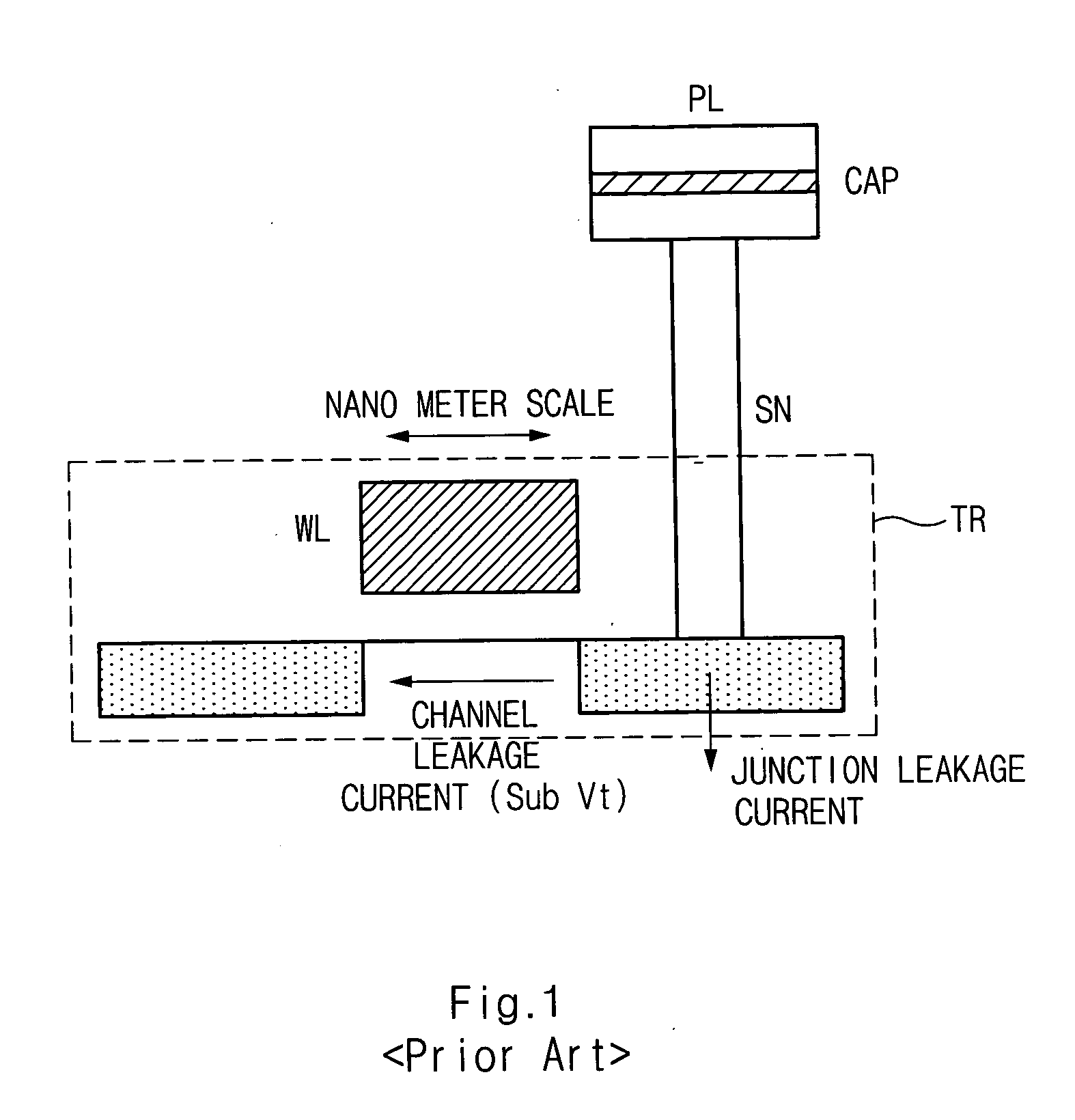
a technology of a memory device and a nanotube cell, which is applied in the field of nanotube cells and memory devices using the same, can solve the problems of junction leakage current generation and difficulty in satisfying the refresh characteristic of the dram cell

Inactive Publication Date: 2005-08-18
SK HYNIX INC
View PDF13 Cites 26 Cited by
  • Summary
  • Abstract
  • Description
  • Claims
  • Application Information

AI Technical Summary

Benefits of technology

[0009] It is an object of the present invention to provide a PNPN nano tube switch through a simple process using a Silicon On Insulator (hereinafter, referred to as “SOI”) wafer in a DRAM.

Problems solved by technology

As a result, it is difficult to satisfy the refresh characteristic of the DRAM cell.
Also, junction leakage current is generated in a storage node terminal which occupies a relatively large area in the DRAM cell.

Method used


Image

  • Nano tube cell and memory device using the same
  • Nano tube cell and memory device using the same
  • Nano tube cell and memory device using the same

Examples


Embodiment Construction

[0032] The present invention will be described in detail with reference to the accompanying drawings.

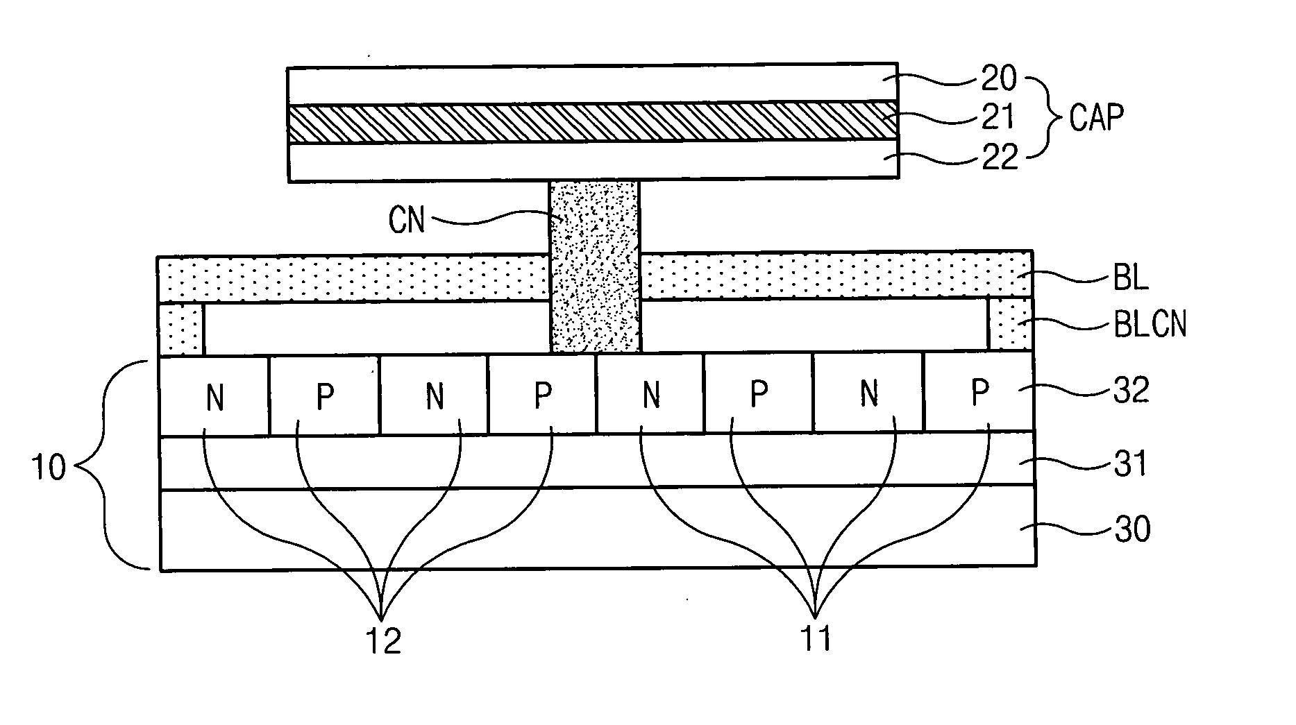
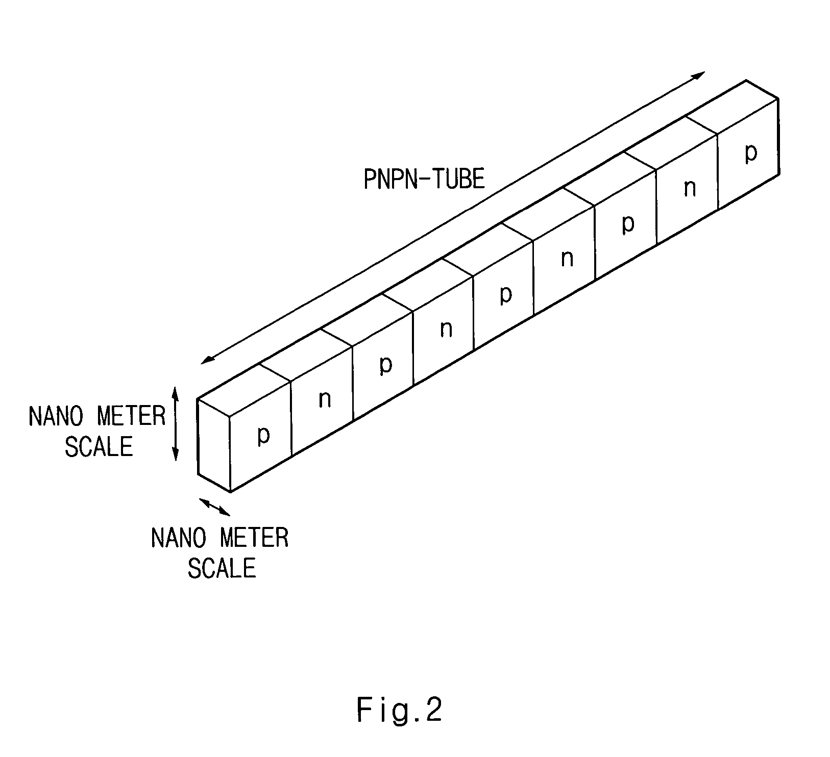
[0033]FIG. 2 is a diagram illustrating the concept of a nano tube cell according to an embodiment of the present invention.

[0034] In an embodiment, the nano tube cell comprises at least two or more of the PNPN diode switches which are connected serially with a tube type. Each of the PNPN diode switch has a nano meter scale in width and in length. In the nano tube cell, leakage current can be reduced regardless of the size of the switch, and the size can be reduced to the atomic level on the scale.

[0035] In the size of the PNPN nano tube switch, the nano meter scale can embodied by distinguishing a P-type region and a N-type region regardless of a short channel characteristic. As a result, a special process is not required.

[0036] Specifically, the whole size of the memory can be reduced by regulating a voltage level applied to the switch device to control on / off operations without...


PUM


Abstract

A nano tube cell and a memory device using the same features a cross point cell using a capacitor and a PNPN nano tube switch to reduce the whole memory size. In the memory device, the unit nano tube cell comprising a capacitor and a PNPN nano tube switch which does not an additional gate control signal is located where a word line and a bit line are crossed, so that a cross point cell array is embodied. As a result, the whole chip size is reduced, and read and write operations are effectively improved.

Description

BACKGROUND OF THE INVENTION [0001] 1. Field of the Invention [0002] The present invention generally relates to a nano tube cell and a memory device using the same, and more specifically, to a technology of reducing the whole memory size by embodying a cross point cell using a capacitor and a PNPN nano tube switch which does not require an additional gate control signal. [0003] 2. Description of the Prior Art [0004]FIG. 1 is a diagram illustrating a conventional DRAM cell. [0005] A conventional DRAM cell comprises a transistor TR and a capacitor CAP which is connected between a plate line PL and one terminal of the transistor TR. The transistor TR performs a switching operation depending on a state of a word line WL to connect the capacitor CAP to a bit line BL. [0006] Here, a switching device of the conventional DRAM cell is a NMOS transistor whose switching operation is controlled by a gate control signal. However, when a cell array is embodied by using the above-described NMOS tra...

Claims


Application Information

Patent Timeline
Patent Type & Authority Applications(United States)
IPC IPC(8): H01L27/108G11C11/24G11C11/401G11C11/54G11C13/02H01L21/8242H01L27/04
CPCB82Y10/00G11C11/54G11C13/003G11C2213/76G11C13/025G11C2213/74G11C13/0033A01B13/02A01B29/00A01B59/043
Inventor KANG, HEE BOK
Owner SK HYNIX INC
Why Eureka
Try Eureka