Cooling apparatus and method for manufacturing liquid crystal display device using the same

Active Publication Date: 2007-07-05
LG DISPLAY CO LTD
View PDF3 Cites 97 Cited by
  • Summary
  • Abstract
  • Description
  • Claims
  • Application Information

AI Technical Summary

Benefits of technology

[0017]A first object of the present invention is to provide a method for manufacturing a liquid crystal display device, which prevents orientation of a liquid crystal layer from being scattered when a sealant is hardened using a liquid crystal drop method.
[00

Problems solved by technology

The liquid crystal injection method requires a long time to inject the liquid crystal, thus reducing productivity as substrate sizes increase.
However, because the sealant layer is hardened under the condition that the liquid crystal layer is formed between the lower and upper substrates, the liquid crystal drop method causes domain defects due to a scattering of the orientation of the liquid

Method used


Image

  • Cooling apparatus and method for manufacturing liquid crystal display device using the same
  • Cooling apparatus and method for manufacturing liquid crystal display device using the same
  • Cooling apparatus and method for manufacturing liquid crystal display device using the same

Examples


Embodiment Construction

[0043]Reference will now be made in detail to embodiments of the present invention, examples of which are illustrated in the accompanying drawings. Wherever possible, the same reference numbers will be used throughout the drawings to refer to the same or like parts.

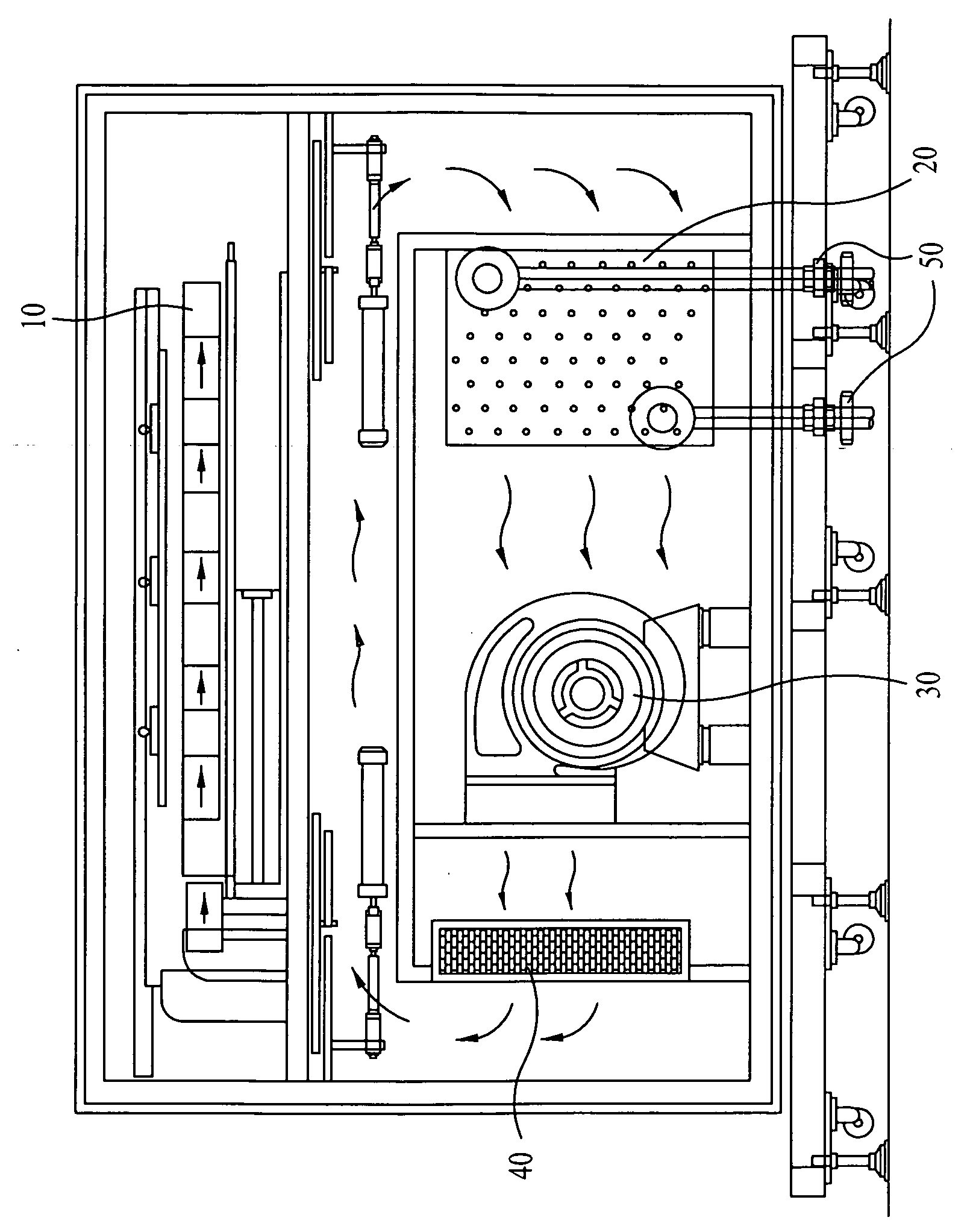
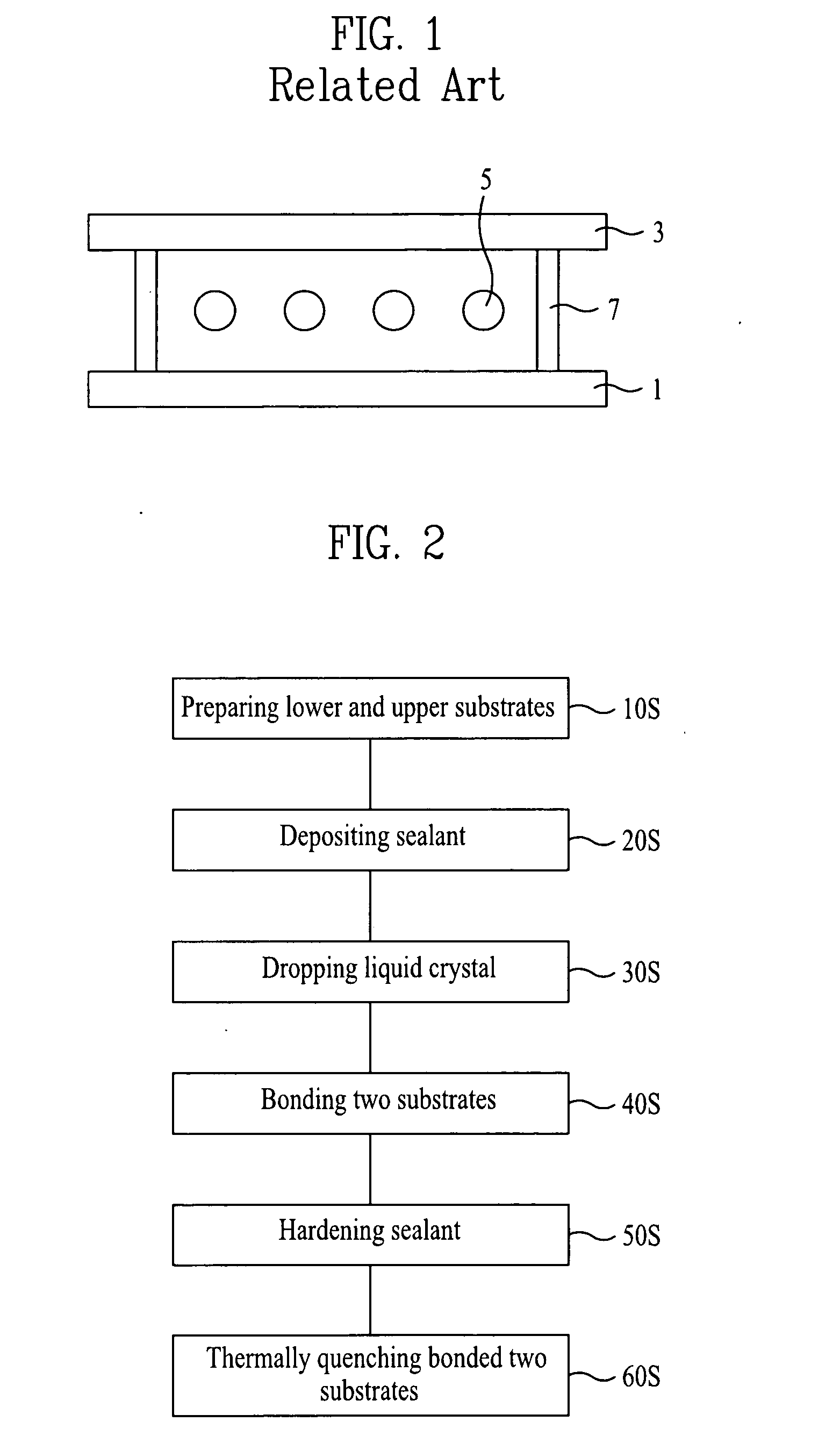
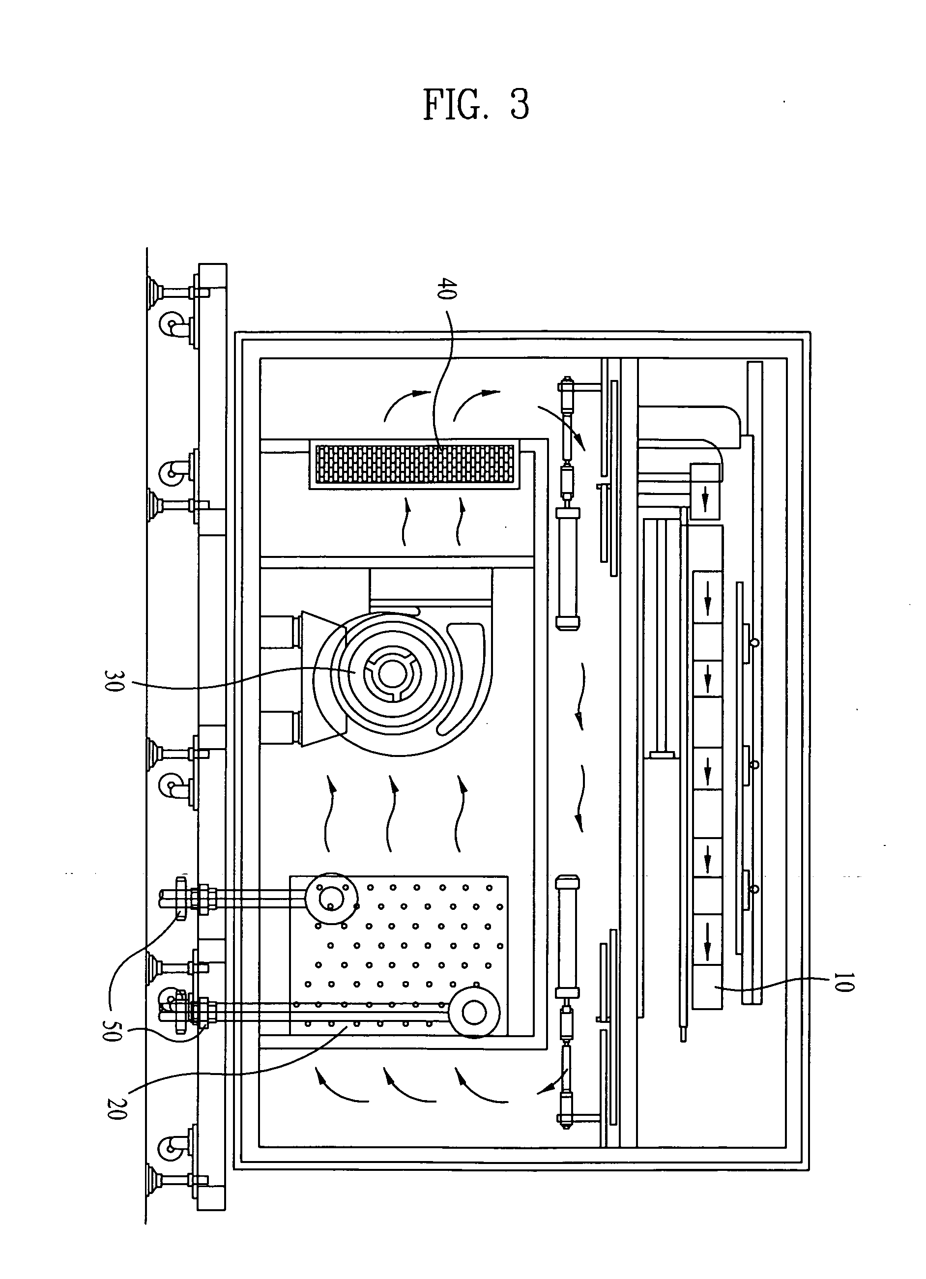
[0044]FIG. 2 is a flow chart illustrating a process for manufacturing a liquid crystal display device in accordance with an embodiment of the present invention.

[0045]First, as illustrated in FIG. 2, a lower substrate and an upper substrate are prepared (10S).

[0046]The lower substrate and the upper substrate are appropriately changed according to the driving mode of a liquid crystal display device.

[0047]That is, when the liquid crystal display device is driven in a Twisted Nematic (TN) mode, gate lines and data lines, which perpendicularly intersect with each other, for defining pixel regions, TFTs formed at the intersections of the gate lines and the data lines and serving as switching elements, and pixel electrodes forme...


PUM

PropertyMeasurementUnit
Temperatureaaaaaaaaaa

Abstract

A method for manufacturing a liquid crystal display device includes preparing a lower substrate and an upper substrate; depositing a sealant on one of the two substrates; dropping a liquid crystal on one of the two substrates; bonding the two substrates to each other; bonding the two substrates to each other by hardening the sealant; and thermal quenching the two bonded substrates. Since thermal quenching of the two bonded substrates is additionally performed after hardening of the sealant is performed using a liquid crystal dropping method, orientation of a liquid crystal layer, which is scattered by the hardening of the sealant, is returned to its original state, thus preventing domain defects.

Description

[0001]This application claims the benefit of Korean Patent Application No. P 2005-0133124, filed Dec. 29, 2005, which is hereby incorporated by reference for all purposes as if fully set forth herein. This application incorporates by reference co-pending application, Ser. No. 10 / 184,096, filed on Jun. 28, 2002 entitled “SYSTEM AND METHOD FOR MANUFACTURING LIQUID CRYSTAL DISPLAY DEVICES FROM LARGE MOTHER SUBSTRATE PANELS” (Attorney Docket Number 8733.666.00); and co-pending application, serial number , filed on Jun. 29, 2006, entitled “METHODS OF MANUFACTURING LIQUID CRYSTAL DISPLAY DEVICES” (Attorney Docket Number 8733.1713.00) for all purposes as if fully set forth herein.BACKGROUND OF THE INVENTION[0002]1. Field of the Invention[0003]The present invention relates to a liquid crystal display (LCD) device, and more particularly, to a method for manufacturing a liquid crystal display device using a liquid crystal drop method.[0004]2. Discussion of the Related Art[0005]A liquid crysta...

Claims


Application Information

Patent Timeline
IPC IPC(8): B32B37/00
CPCG02F1/1341G02F1/1333
Inventor SHIN, JAE HO
Owner LG DISPLAY CO LTD
Why Eureka
Try Eureka