

Micro electro mechanical system, semiconductor device, and manufacturing method thereof
- Summary
- Abstract
- Description
- Claims
- Application Information
AI Technical Summary
Benefits of technology
Problems solved by technology
Method used
Image

Examples
embodiment modes
[0041] Hereinafter, the embodiment modes of the present invention will be described with reference to the accompanying drawings. It is easily understood by those skilled in the art that modes and details herein disclosed can be modified in various ways without departing from the spirit and the scope of the present invention. It should be noted that the present invention should not be interpreted as being limited to the description of the embodiment modes to be given below. Note that in all drawings showing the embodiment modes, the same reference numerals are used for the same portions or the portions having the same functions, and description thereof is omitted.
embodiment mode 1
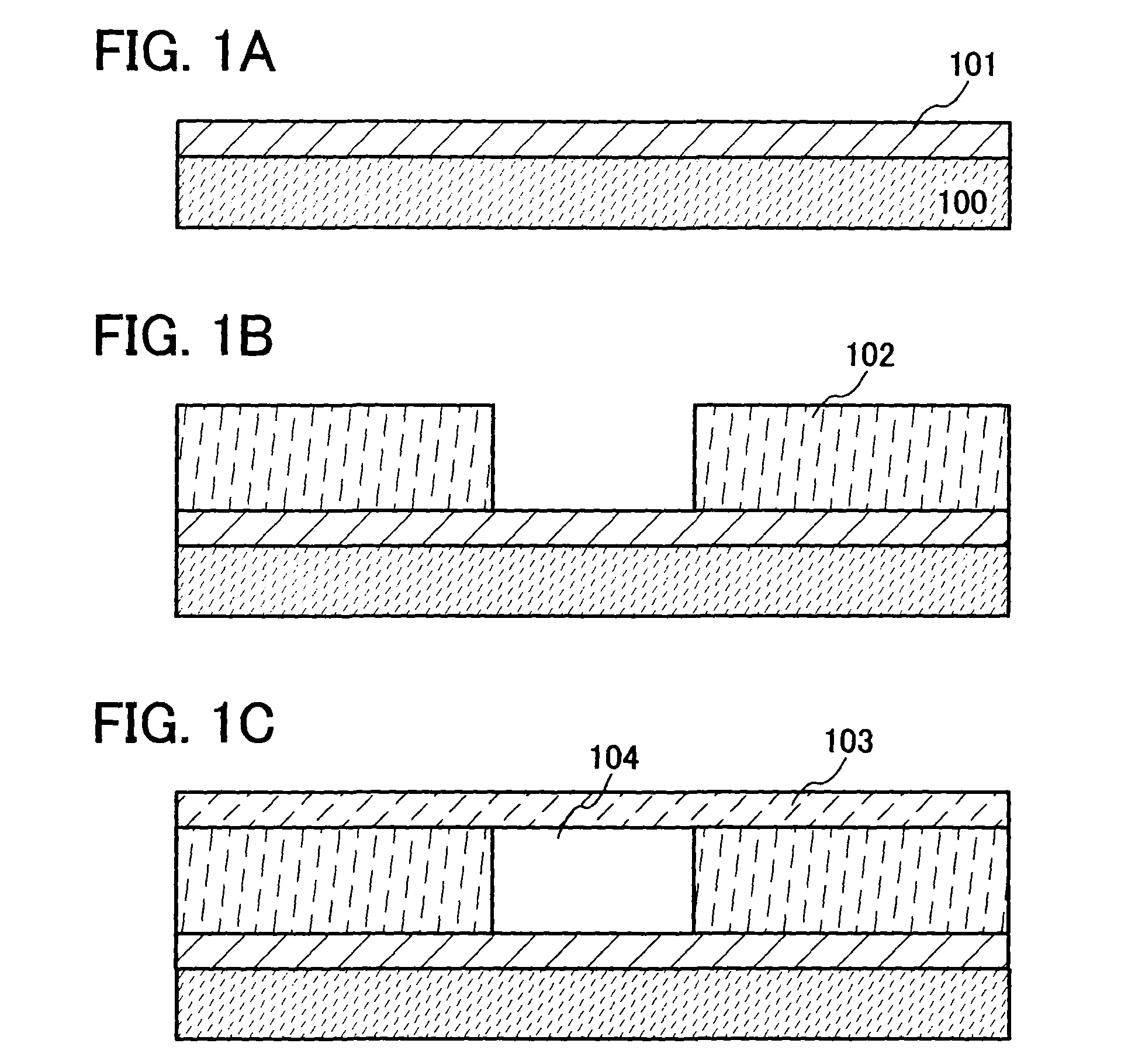
[0042] Embodiment Mode 1 will describe a manufacturing process of a micro electro mechanical system in which an interspace is formed by using spacer layers.
[0043] A substrate 100 is prepared as shown in FIG. 1A. As the substrate 100, a substrate having an insulating surface (also referred to as an insulating substrate) such as a glass substrate, a quartz substrate, or a plastic substrate can be used. For example, when a plastic substrate is used, a highly flexible and lightweight micro electro mechanical system can be provided. In addition, a thin micro electro mechanical system can be provided by thinning a glass substrate by grinding and polishing, and so on. Further, a conductive substrate such as metal or a semiconductor substrate such as silicon can be used as the substrate 100. An insulating layer can be formed on a surface of such a substrate to be used.
[0044] A layer having an element which has a particular function (hereinafter, also referred to as a first functional laye...
embodiment mode 2
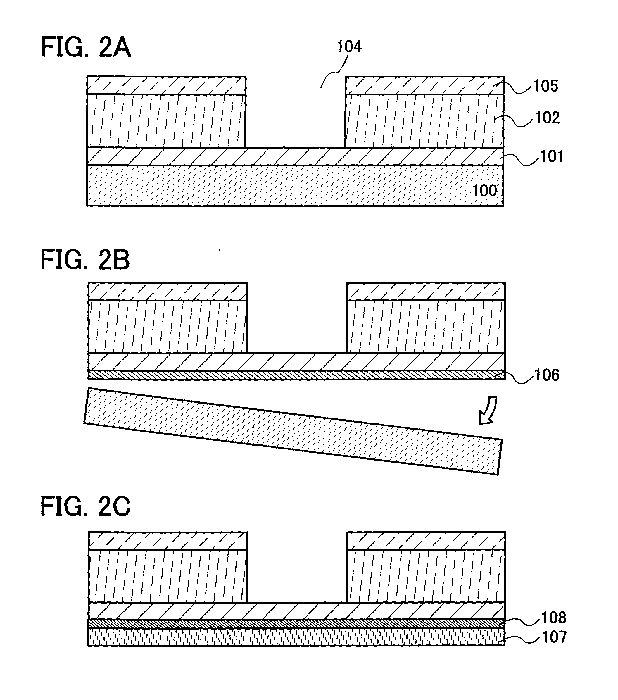
[0060] Embodiment Mode 2 will describe another structure of a micro electro mechanical system in which an interspace is formed by a spacer layer.
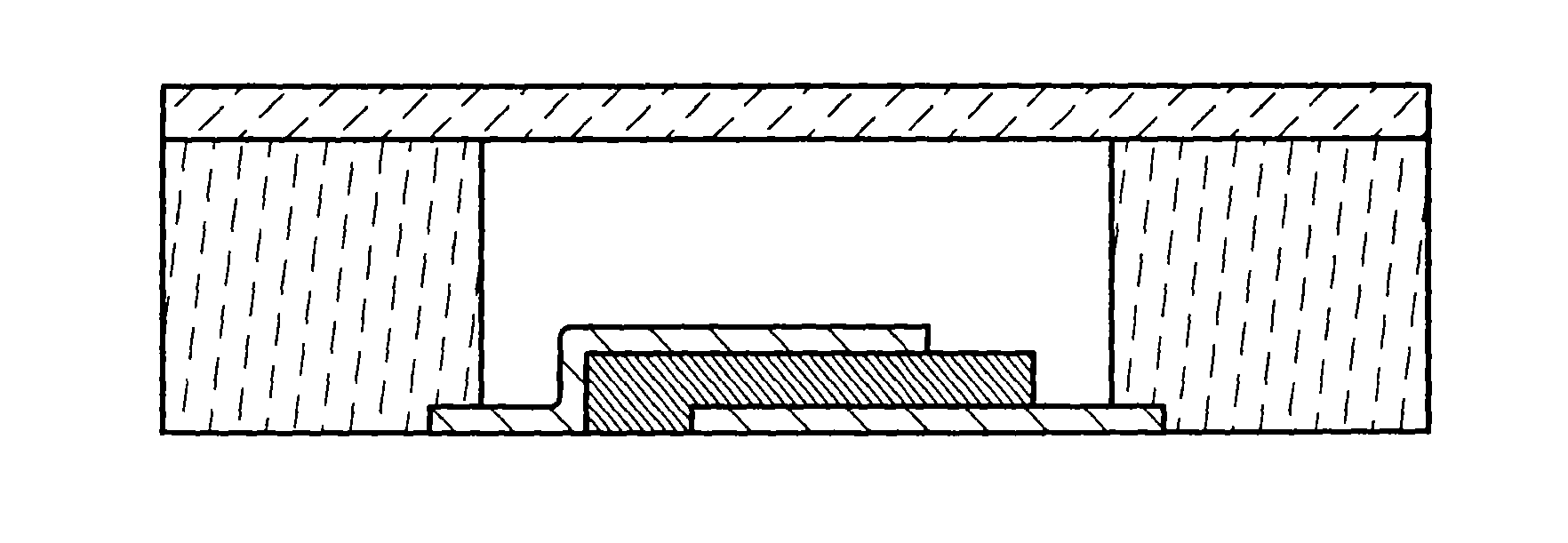
[0061]FIG. 2A shows a micro electro mechanical system having another structure, and is different from the micro electro mechanical system shown in FIG. 1C in that a sealing substrate 105 provided with an opening portion is formed. The other structures are the same as in FIG. 1C and thus, description thereof is omitted. The opening portion of the sealing substrate 105 has almost the same form as the opening portion provided in the spacer layer so as to be overlapped. In other words, the interspace 104 is surrounded by the first functional layer 101 on its bottom side, the spacer layer 102 and the sealing substrate 105 on its lateral side, and its top layer side is open. Like this, the form of the interspace is not necessarily closed.
[0062] Here, the explanations of the first functional layer 101 and the spacer layer 102 in the Embodiment M...
PUM
| Property | Measurement | Unit |
|---|---|---|
| Adhesivity | aaaaa | aaaaa |
Abstract
Description
Claims
Application Information