Matching network

a technology of matching network and switch, applied in the field of matching network, can solve the problems that the switch can be mechanically integrated into the matching network particularly unproblematically, and achieve the effect of very fast switch, good or best possible antenna matching, and wearless

Inactive Publication Date: 2007-07-05
INFINEON TECH AG
View PDF3 Cites 58 Cited by
  • Summary
  • Abstract
  • Description
  • Claims
  • Application Information

AI Technical Summary

Benefits of technology

[0033] In a further preferred embodiment, the control means is implemented to set a plurality of states of the matching network by switching the CMOS switch, when the control means determines that the impedance matching at the input port is worse than a predetermined threshold. The control means is further implemented to determine further information for the plurality of states of the matching network, how good impedance matching is at the input port of the matching network for the plurality of states. Further, the control means is implemented to select a new state of the matching network based on the further information. Such an implementation of the control unit is particularly advantageous when the matching network comprises a plurality of CMOS switches, so that more than two matching states can be selected for the matching network. Thereby, it can be achieved that the control means identifies, for example, the best of several possible matching states of the matching network in that the control means sets the several matching states in a predetermined sequence and then determines how good the matching in the respective matching states actual...

Problems solved by technology

Further, the CMOS switch can be integrated mechanically into a matching network parti...

Method used


Image

  • Matching network
  • Matching network
  • Matching network

Examples


first embodiment

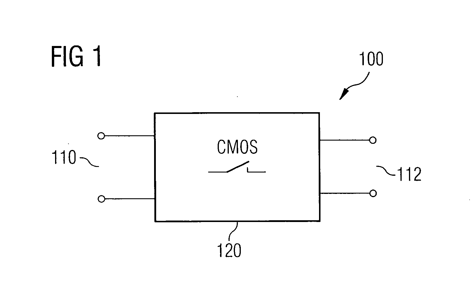
[0050]FIG. 1 shows a schematic illustration of an inventive matching network according to the present invention. The matching network of FIG. 1 is designated by 100 in its entirety and has an input port 110 for receiving high-frequency power as well as an output port 112. The matching network comprises a switchable impedance transformation circuit 120, which is connected between the input port and the output port. In a high-frequency path, the impedance transformation circuit 120 comprises a CMOS switch, which has a first switching state and a second switching state. In the first switching state, for example, a CMOS switch is closed or low-resistively conductive, while in the second switching state, the CMOS switch is opened or high-resistive, respectively. The impedance transformation circuit 120 (also referred to as impedance transformation network) is further implemented to match a (given) first impedance applied to the output port on the input side to a first predetermined imped...

second embodiment

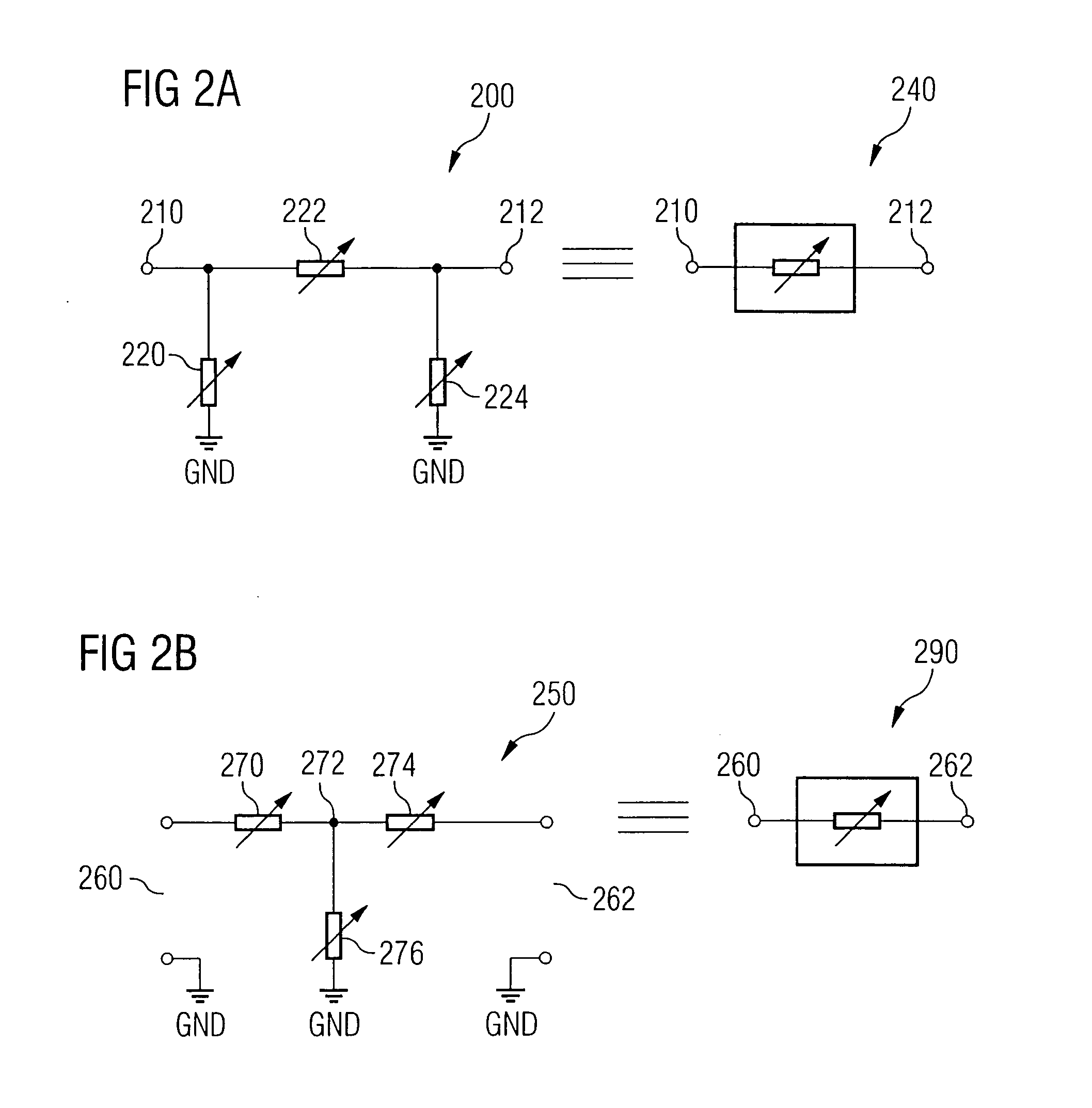
[0055]FIG. 2a shows a circuit diagram of the inventive matching network according to the present invention. The matching network shown in FIG. 2a is designated by 200 in its entirety. The matching network 200 has a π switching configuration. The matching network 200 has an input port 210 as well as an output port 212. In the shown embodiment, the signals applied to the input port 210 and the output port 212 are related to a reference potential GND. In other words, the input port 210 and the output port 212 form unbalanced ports. A first adjustable impedance element 220 (also referred to as impedance transformation element or briefly element) is connected between the input port 210 (or a conductor of the input port, respectively) and the reference potential GND. A second adjustable impedance element 222 is connected between the input port 210 and the output port 212. A third adjustable impedance element 224 is further connected between the output port 212 (or a conductor of the outpu...

third embodiment

[0061]FIG. 2b shows further a circuit diagram of an inventive matching network according to the present invention. The matching network of FIG. 2b is designated by 250 in its entirety. The matching network 250 has an input port 260 and an output port 262, which are here both exemplarily shown as unbalanced ports, with regard to a reference potential GND. An adjustable impedance element 270 is connected between a terminal of the input port 260 and a central node 272. A second adjustable impedance element 274 is further connected between the center node 272 and the terminal of the output port 262. Further, a third adjustable impedance element 276 is connected between the center node 274 and the reference potential GND. Thus, the three adjustable impedance elements 270, 274, 276 form a T circuit, which is connected between the input port 260, the output port 262 and the reference potential GND. The matching network 250 can also be described by a schematic illustration 290.

[0062] It sho...


PUM


Abstract

A matching network for matching an antenna to a transmitter or receiver comprises an input port for receiving high-frequency power, an output port and a switchable impedance transformation circuit, which is connected between the input port and the output port. The impedance transformation circuit comprises a CMOS switch in a high-frequency path, which has a first switching state and a second switching state. The impedance transformation circuit is implemented to match a first impedance applied to the output port to a first predetermined impedance in the first switching state, and to match a second impedance applied to the output port to a second predetermined impedance in the second switching state. The inventive matching network allows a particularly good utilization of power provided by a transmitting amplifier or an antenna.

Description

Cross-Reference to Related Application [0001] This application claims priority from German Patent Application No. 102005058875.1, which was filed on Dec. 9, 2005 and is incorporated herein by reference in its entirety. BACKGROUND OF THE INVENTION [0002] 1. Field of the Invention [0003] The present invention relates generally to a matching network for matching an antenna to a transmitter or receiver, and particularly to a dynamic matching network for multi-band antennas. [0004] 2. Description of the Related Art [0005] Wireless communication units are nowadays used in a plurality of applications, to allow communication between a wireless means and a stationary means or also between several wireless means. [0006] One of the most important characteristics of modern wireless communication units is their operating time, which is divided into the so-called “talk time” and the so-called “stand time”. The mentioned characteristics are influenced by antenna matching in a front end or high-fre...

Claims


Application Information

Patent Timeline
IPC IPC(8): H03C1/52H04B1/02
CPCH03H7/40
Inventor HEUERMANN, HOLGERSADEGHFAM, ARASH
Owner INFINEON TECH AG
Why Eureka
Try Eureka