Tuneable delay line

a delay line and tuneable technology, applied in the direction of delay lines, waveguides, electrical devices, etc., can solve the problems of large components, difficult integration with standard semiconductor technologies, and the majority of modern tuneable delay lines are quite power-consuming, and achieve low power consumption, long delay times, and small size

Inactive Publication Date: 2007-07-12
HIGHBRIDGE PRINCIPAL STRATEGIES LLC AS COLLATERAL AGENT
View PDF7 Cites 9 Cited by
  • Summary
  • Abstract
  • Description
  • Claims
  • Application Information

AI Technical Summary

Benefits of technology

[0004] Hence, as described above, there is a need for a tuneable delay line which is of a small size, has low power consumption, and capable of having long delay times.

Problems solved by technology

Most technologies used in delay lines result in bulky components, which are usually not cost-effective and are difficult to integrate with standard semiconductor technologies.
In addition, most contemporary tuneable delay lines are quite power consuming, which is usually a drawback.

Method used


Image

  • Tuneable delay line
  • Tuneable delay line
  • Tuneable delay line

Examples


embodiment 500

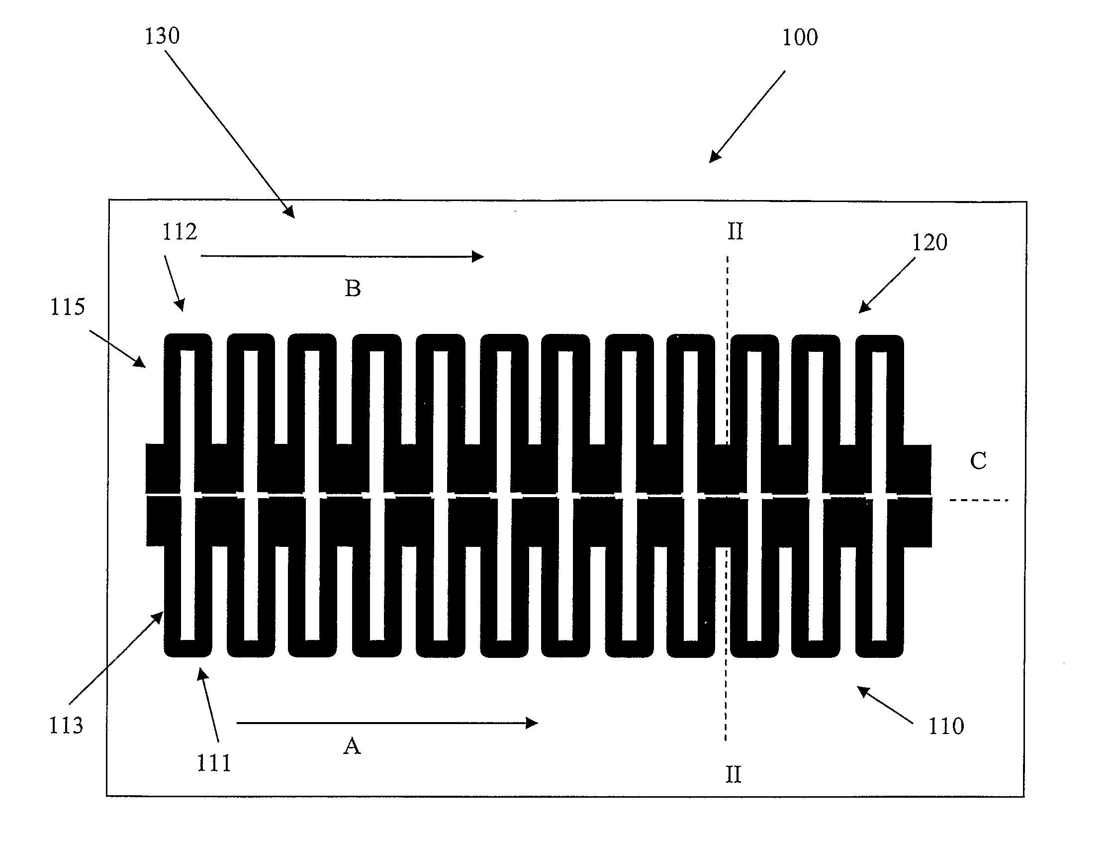
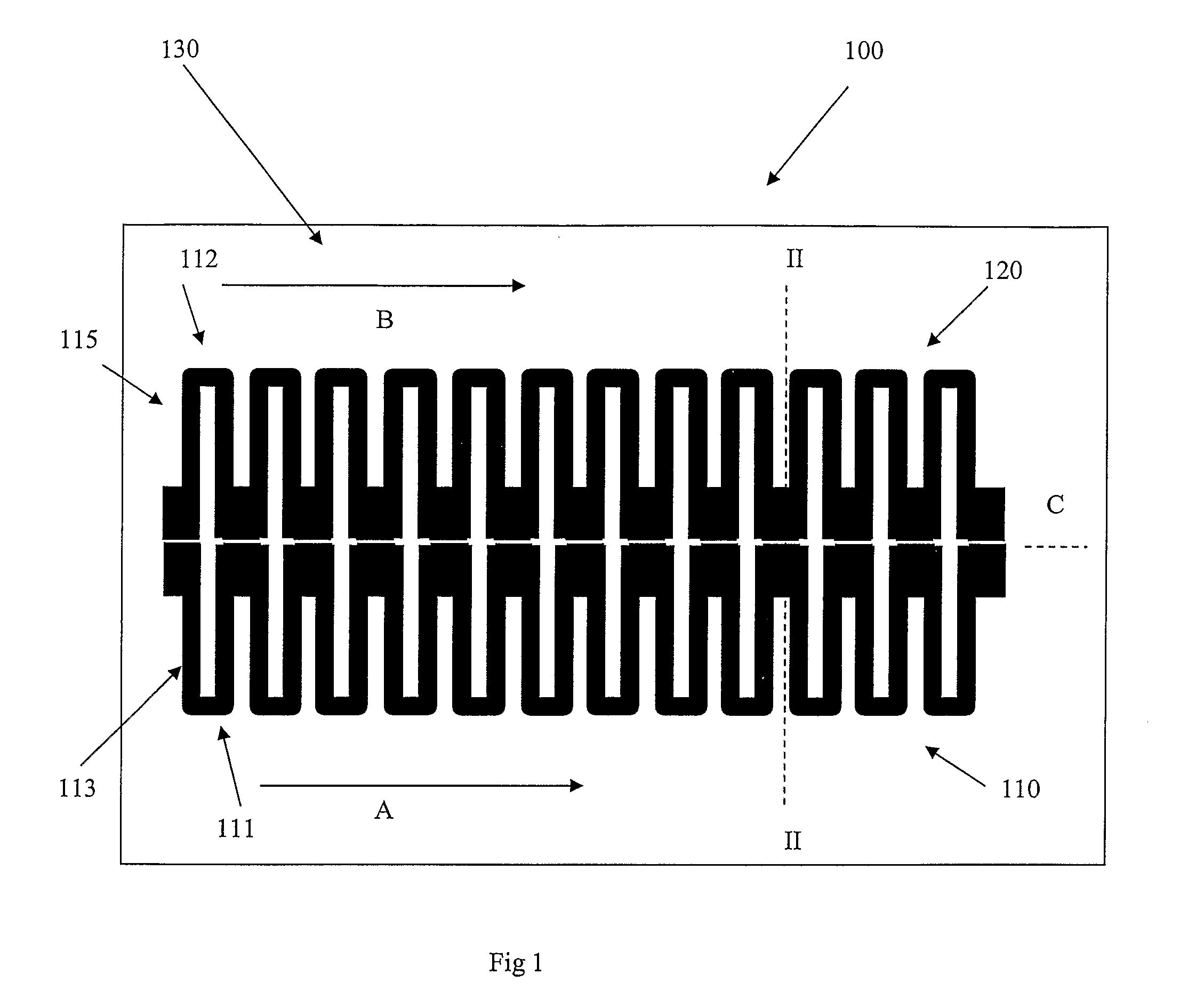
[0030] Yet a further embodiment 500 of a device according to the invention is shown in FIGS. 5a-5c. This embodiment shows a way of decreasing the ohmic losses: a first conducting pattern, a delay line 505, shown in FIG. 5c, is formed in the bottom layer of the device, i.e. between a substrate and a ferroelectric material, the first delay line 505 being essentially similar to those shown in FIGS. 1 and 3, i.e. it has two meander shaped conductors 510, 520, essentially parallel to each other, extending in a common general direction, which conductors are essentially each other's mirror image with respect to an imagined line C between them, said imagined line extending in the general direction of the device.

[0031] Thus, the two conductors of the delay line 505 have one section 532 that points “straight ahead”, i.e. in the general direction of the device, and then one section 531 that is perpendicular to the general direction C of the device 500. Both conductors 510, 520, have alternatin...

embodiment 700

[0035]FIG. 7 shows an embodiment 700 of the invention which will alleviate the problem of mutual negative coupling between the strips: the device comprises a first 710 and a second 720 conducting pattern, arranged on different sides of the ferroelectric layer. Each of the conducting patterns alternatingly comprises sections arranged at 45 degrees or negative 45 degrees, with respect to the general direction C of the device. However, if the first section 721 of the first conductor is arranged at 45 degrees, the first section 713 of the second conductor will be arranged at negative 45 degrees, the two conductors being arranged so that sections which point in different directions intersect each other. Due to the geometry of this, the sections will intersect each other at an angle of 90 degrees, which will essentially eliminate the negative magnetic coupling between the strips.

[0036] In a more generalized sense, the embodiment shown in FIG. 7 could be described in the following way: The...

embodiment 1200

[0043]FIGS. 12a and 12b show top views of components in another embodiment 1200 of the invention, and FIG. 12c shows the embodiment 1200 as a whole in a top view. This embodiment may give even further reduced losses and increased process tolerances, and uses a capacitance which reduces the required bias voltage, at the same time as it eliminates the floating ground in the middle.

[0044]FIG. 12a shows the bottom layer, and FIG. 12b shows the top layer, both layers being conducting, and separated in the same manner as the conductors in the embodiments shown in FIGS. 7-11.

[0045] The bottom conductor 12a and the top conductor 12b are of essentially the same design, and intended to be arranged “on top of each other”, with the mentioned separating layers between them, in such a manner that corresponding parts in each conductor “cover” each other. Each conductor comprises two meander shaped conducting patterns, being arranged to be each other's mirror image with respect to an imaginary lin...


PUM


Abstract

A tunable electromagnetic delay line, comprising a first conductor with a first main direction of extension, said first conductor being arranged on top of a non-conducting substrate, characterized in that the delay line additionally comprises a layer of a ferroelectric material with first and second main surfaces, which layer separates the first conductor and the substrate, and in that the delay line also comprises a second conductor with a second main direction of extension, with the first and second main directions of extensions essentially coinciding with each other, and with the first and second conductors being each other's mirror image with respect to an imagined line in the center of the delay line along said first and second main directions of extension, said tuning being accomplished by applying a voltage between said first and second conductors.

Description

TECHNICAL FIELD [0001] The present invention relates to a tunable electromagnetic delay line, comprising a first conductor with a first main direction of extension, said first conductor being arranged on top of a non-conducting substrate. BACKGROUND ART [0002] Delay lines are a common component in many contemporary electrical systems, usually microwave systems. Examples that could be mentioned of fields of technology where delay lines are used are radar systems, amplifiers and oscillators. [0003] Most technologies used in delay lines result in bulky components, which are usually not cost-effective and are difficult to integrate with standard semiconductor technologies. Moreover, it is quite desirable for a delay line to be tuneable, i.e. to have a delay time which can be altered. In addition, most contemporary tuneable delay lines are quite power consuming, which is usually a drawback. DISCLOSURE OF THE INVENTION [0004] Hence, as described above, there is a need for a tuneable delay...

Claims


Application Information

Patent Timeline
Patent Type & Authority Applications(United States)
IPC IPC(8): H01P1/18H01P9/00
CPCH01P9/04H01P9/006
Inventor KUYLENSTIERNA, DAN
Owner HIGHBRIDGE PRINCIPAL STRATEGIES LLC AS COLLATERAL AGENT
Why Eureka
Try Eureka