Common transparent electrode for reduced voltage displays

a transparent electrode and display technology, applied in static indicating devices, instruments, non-linear optics, etc., can solve the problems of increased thickness of displays, higher system costs, and increased cost, so as to reduce the total brightness and contrast of devices, reduce thickness, and reduce the effect of adding the minimum of complexity

Inactive Publication Date: 2007-07-12
IND TECH RES INST
View PDF26 Cites 15 Cited by
  • Summary
  • Abstract
  • Description
  • Claims
  • Application Information

AI Technical Summary

Benefits of technology

[0012] The present invention includes several advantages, not all of which are incorporated in a single embodiment. The present invention, through the use of a common electrode located between liquid crystal layers, which are, in turn, located between patterned electrodes, cuts the erase voltage requirement in half, without substantially reducing the total brightness and contrast of the device, as occurs if one simply reduces the thickness of liquid crystal or absorber layer interposed between the addressable row and column electrodes. The current invention achieves these goals with a minimum of added complexity thus maintaining display brightness and contrast while greatly reducing system cost.

Problems solved by technology

These displays suffer from the added thickness due to the polymer host and the absorber layer disposed between the row and column electrodes.
Higher drive voltages in turn lead to higher system costs.
These displays require multiple transparent substrates leading to higher cost, thicker less flexible displays and require separate drive signals for each imaging layer.
Although this is desirable when addressing full color displays, the requirement of alternating electrodes adds to the number of independent driver signals required, the number of connections required and increases the complexity of fabrication, all leading to higher system costs.
These displays also lack the interposed absorbing layer between the electrodes thus reducing the effectiveness of a contrasting absorber layer.
These displays also suffer from having multiple supports.
This disclosure also suffers from having multiple supports in the line of sight through the device.
Although this is desirable when addressing full color displays the requirement of alternating electrodes adds to the number of independent driver signals required, the number of connections required and increases the complexity of fabrication all leading to higher system costs.
These displays also lack the interposed absorbing layer between the electrodes thus reducing the effectiveness of the contrasting absorber layer.

Method used


Image

  • Common transparent electrode for reduced voltage displays
  • Common transparent electrode for reduced voltage displays
  • Common transparent electrode for reduced voltage displays

Examples


example 1

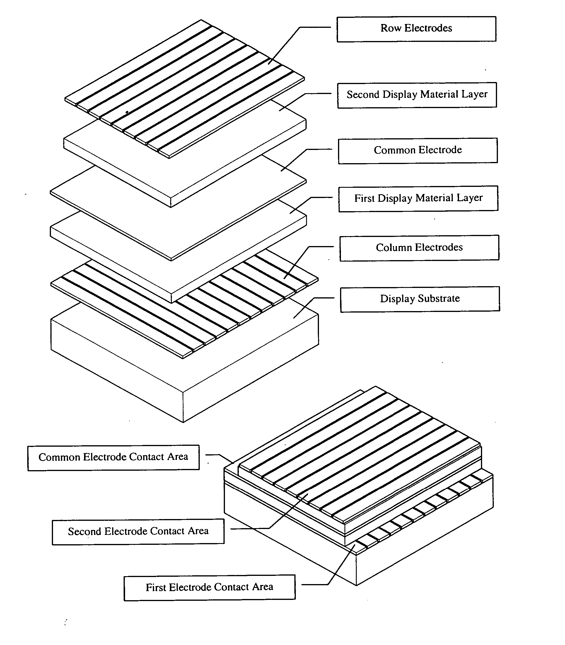
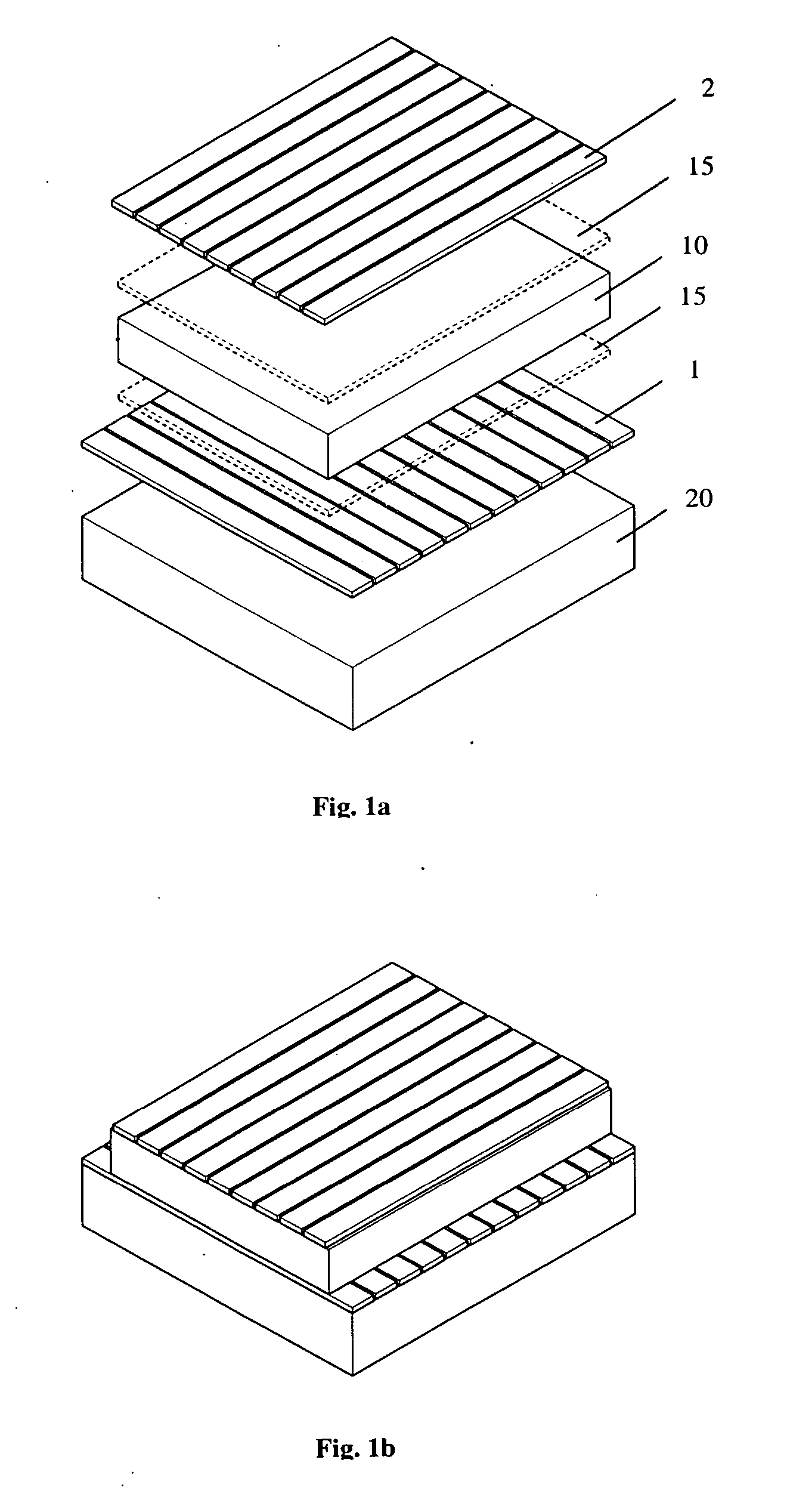
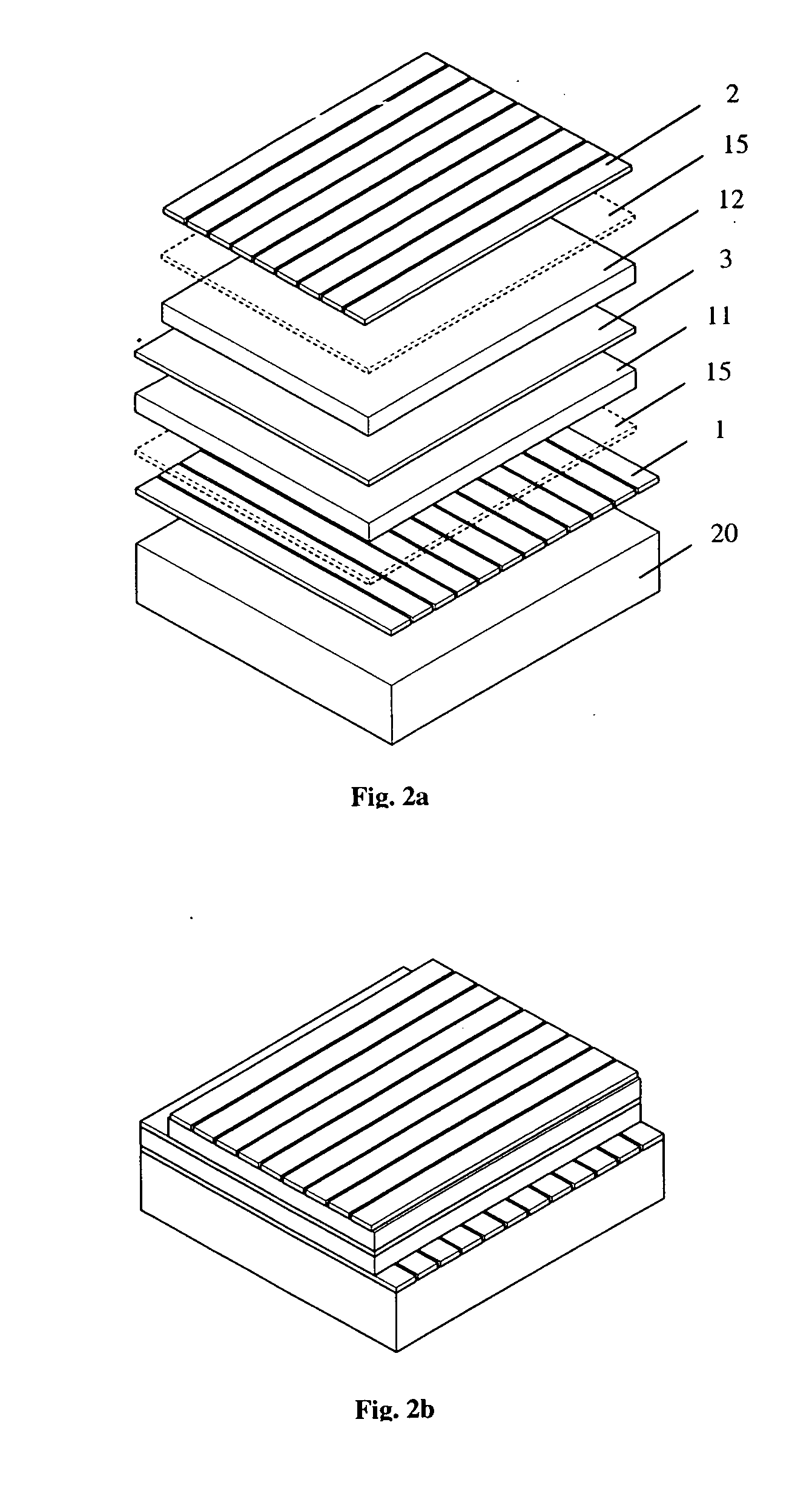
Two Imaging Layers with an Intervening Common Electrode

[0121] An experiment was performed to examine the effects of adding a conductive layer to the top of the chiral nematic liquid crystal. The emulsion was prepared using cholesteric liquid crystal oil MERCK BL118, available from E.M. Industries of Hawthorne, N.Y. U.S.A. by limited coalescence in accordance with the procedure described in U.S. Pat. No. 6,556,262 to Stephenson.

[0122] For an emulsion having domain size of approximately 10 microns, the following procedure was used: The emulsions were made by first preparing BL118 slurry. A solution of 230 gms of distilled water, 103.5 gms BL118, 3.41 gms LUDOX® M50, and 7.12 gms of MAE adipate. Simultaneously, a solution of MAE adipate consisting of 2.0 gms MAE adipate and 18 gms distilled water. The solutions were added together, heated to 50C, and mixed with a high shear Silverson mixer at 5000 rpm for 2 minutes. The solution is then passed through a Microfluidizer twice at 3000 p...


PUM

PropertyMeasurementUnit
AC voltageaaaaaaaaaa

Abstract

The present invention relates to a display comprising, in order, a support, a first patterned conductor, a first level of electrically modulated imaging material, a coextensive common electrode conductor, a second level of electrically modulated imaging material, and a second patterned conductor and a method of imaging the display.

Description

FIELD OF THE INVENTION [0001] The present invention relates to a structure and drive scheme to more efficiently image bistable displays. BACKGROUND OF THE INVENTION [0002] Displays comprising a transparent substrate, transparent electrodes disposed on the substrate, a polymer dispersed cholesteric liquid crystal disposed over the transparent electrodes, a contrasting absorbing layer disposed over the liquid crystal layer and printed top electrodes have been described as, for example, in U.S. Pat. No. 6,788,362 and references therein. These displays have several advantages over displays having liquid crystal layers disposed between multiple glass or plastic supports and displays having multiple stacked transparent electrodes with alternating patterns of rows and columns. These advantages include ease of manufacture, lower cost and more flexible designs. [0003] Bistable cholesteric liquid crystal displays have advantages over more conventional liquid crystal displays in that they do n...

Claims


Application Information

Patent Timeline
Patent Type & Authority Applications(United States)
IPC IPC(8): G02F1/1347
CPCG02F1/133G02F1/134309G09G3/3629G02F1/13306G09G2300/0486G09G2310/061G09G2300/023
Inventor BURBERRY, MITCHELL S.RANKIN, CHARLES M. JR.RICKS, THEODORE K.
Owner IND TECH RES INST
Why Eureka
Try Eureka