Memory device, memory circuit and semiconductor integrated circuit having variable resistance

a memory circuit and integrated circuit technology, applied in semiconductor devices, digital storage, instruments, etc., can solve the problems of increasing recording/reproduction errors, s/n deterioration, etc., and achieves short rewritable life, long write time, and high write power

Active Publication Date: 2007-07-12
PANASONIC CORP
View PDF9 Cites 57 Cited by
  • Summary
  • Abstract
  • Description
  • Claims
  • Application Information

AI Technical Summary

Benefits of technology

[0008] A transistor having a source, a drain and a gate is formed on a semiconductor substrate. A protective insulating layer is formed over the transistor. A conductive layer is formed on the protective insulating layer. A variable resistance layer made of the variable-resistance material is formed on the conductive layer. Two electrodes are formed on the variable resistance layer. A contact plug for electrically connecting one of the drain and source of the transistor to the conductive layer is provided.
[0009] In this memory device, an application of an electrical pulse between the electrodes and the conductive layer changes the resistance values of portions (variable resistance portions) of the variable resistance layer located directly under the respective electrodes. In this manner, the variable resistance portions have a plurality of resistance states. If the respective resistance states are associated with numerical values, one bit or multiple bits of information can be stored. In addition, the transistor serves as a switch, so that the memory device is used as a memory cell.
[0010] With this memory device, a nonvolatile solid-state memory device without drawbacks such as high write power, long write time, short rewritable life and difficulty in increasing the capacity (device miniaturization), which are drawbacks in conventional nonvolatile solid-state memory devices, is implemented.
[0011] According to still another aspect of the present invention, a memory circuit includes: a first memory block; a second memory block; and a first block-selecting transistor. The first memory block is connected between a first node and a second node. The first block-selecting transistor is connected in series with the first memory block between the first node and the second node. The second memory block is connected between a third node and an interconnect node connecting the first memory bl...

Problems solved by technology

However, in the memory LSI with the cross-point structure shown in FIG. 16, electrical pulses applied during recording affect memory cells other than the memory cell at the intersection of a selected bit line BL and a selected plate line PL and, during reproductio...

Method used


Image

  • Memory device, memory circuit and semiconductor integrated circuit having variable resistance
  • Memory device, memory circuit and semiconductor integrated circuit having variable resistance
  • Memory device, memory circuit and semiconductor integrated circuit having variable resistance

Examples


embodiment 1

Configuration of Memory Device

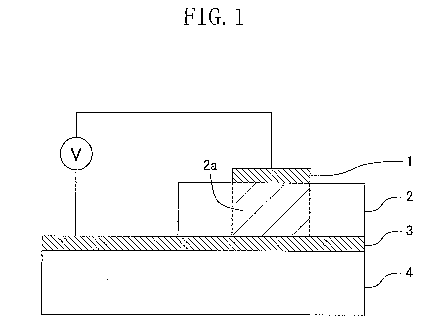
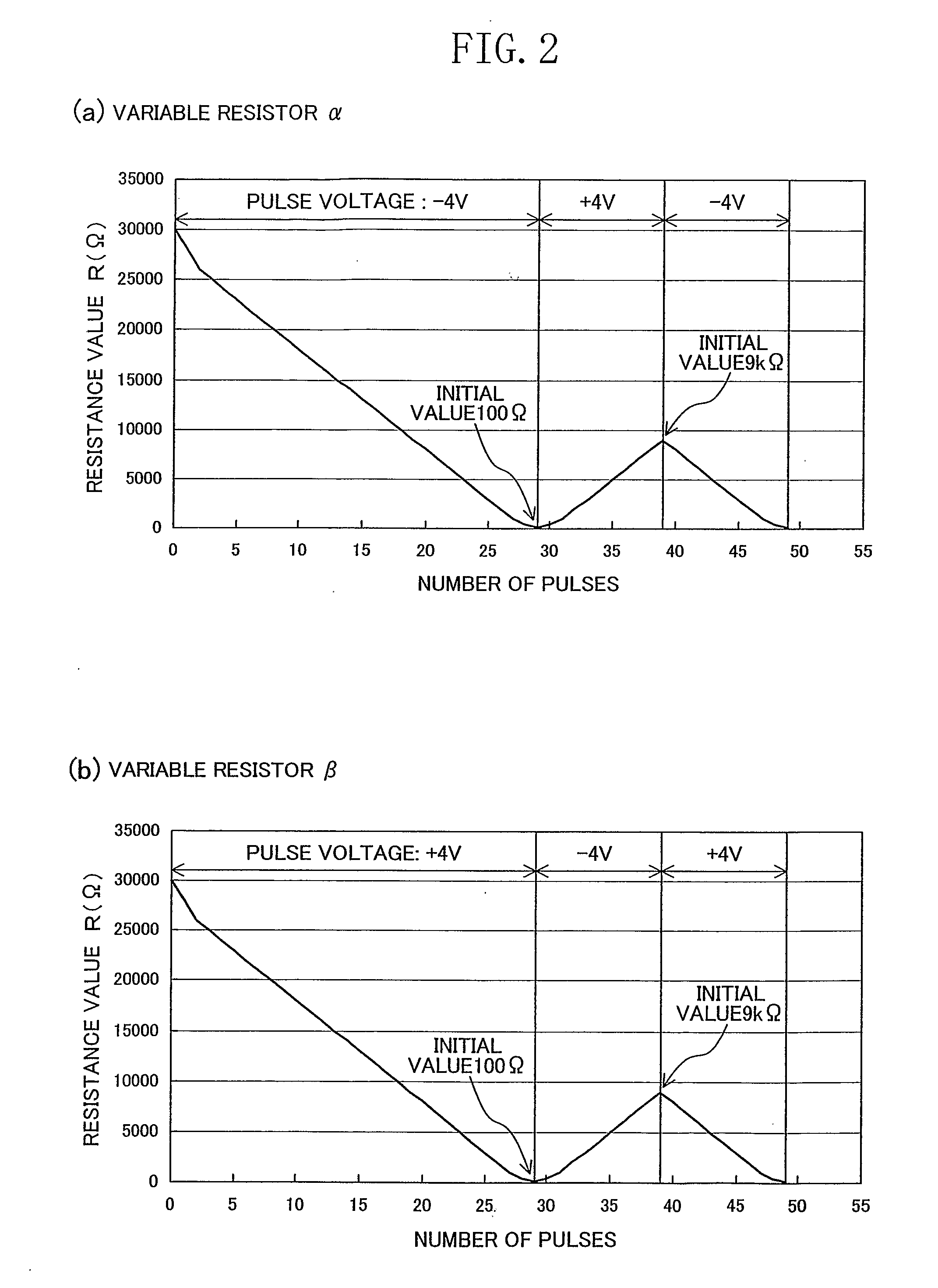
[0049]FIG. 4(a) shows a configuration of a memory device according to a first embodiment of the present invention. In the memory device, variable resistors 5 and 6 whose resistance values vary depending on the polarity of an electrical pulse applied thereto are connected in series between a power supply terminal 7 and a power supply terminal 8. An input / output terminal 9 is connected to an interconnect node connecting the variable resistors 5 and 6. The variable resistor 5 has its initial resistance value set at 100 Ω through the initialization process described with reference to FIGS. 2 and 3. The resistance value of the variable resistor 5 increases when a pulse voltage for setting the input / output terminal 9 to positive is applied between the input / output terminal 9 and the power supply terminal 7 whereas the resistance thereof value decreases when a pulse voltage for setting the input / output terminal 9 to negative is applied. The variable resistor ...

embodiment 2

Configuration of Memory Device

[0057]FIG. 7(a) shows a configuration of a memory device according to a second embodiment of the present invention. A variable resistor 6 in this memory device has its initial resistance value set at 9 kΩ through the initialization process described with reference to FIGS. 2 and 3. The resistance value of the variable resistor 6 decreases when a pulse voltage for setting a power supply terminal 8 to positive is applied between the power supply terminal 8 and an input / output terminal 9 and the resistance value thereof increases when a pulse voltage for setting the power supply terminal 8 to negative is applied. The other part of the configuration is similar to that shown in FIG. 4(a).

Recording of Information in Memory Device

[0058] To record information in this memory device, as shown in FIG. 7(a), a recording pulse voltage having a positive pulse (voltage: +2V and pulse width: 10 ns) and a negative pulse (voltage: −2V and pulse width: 10 ns) is applie...

embodiment 3

Circuit Configuration of Memory Array Circuit

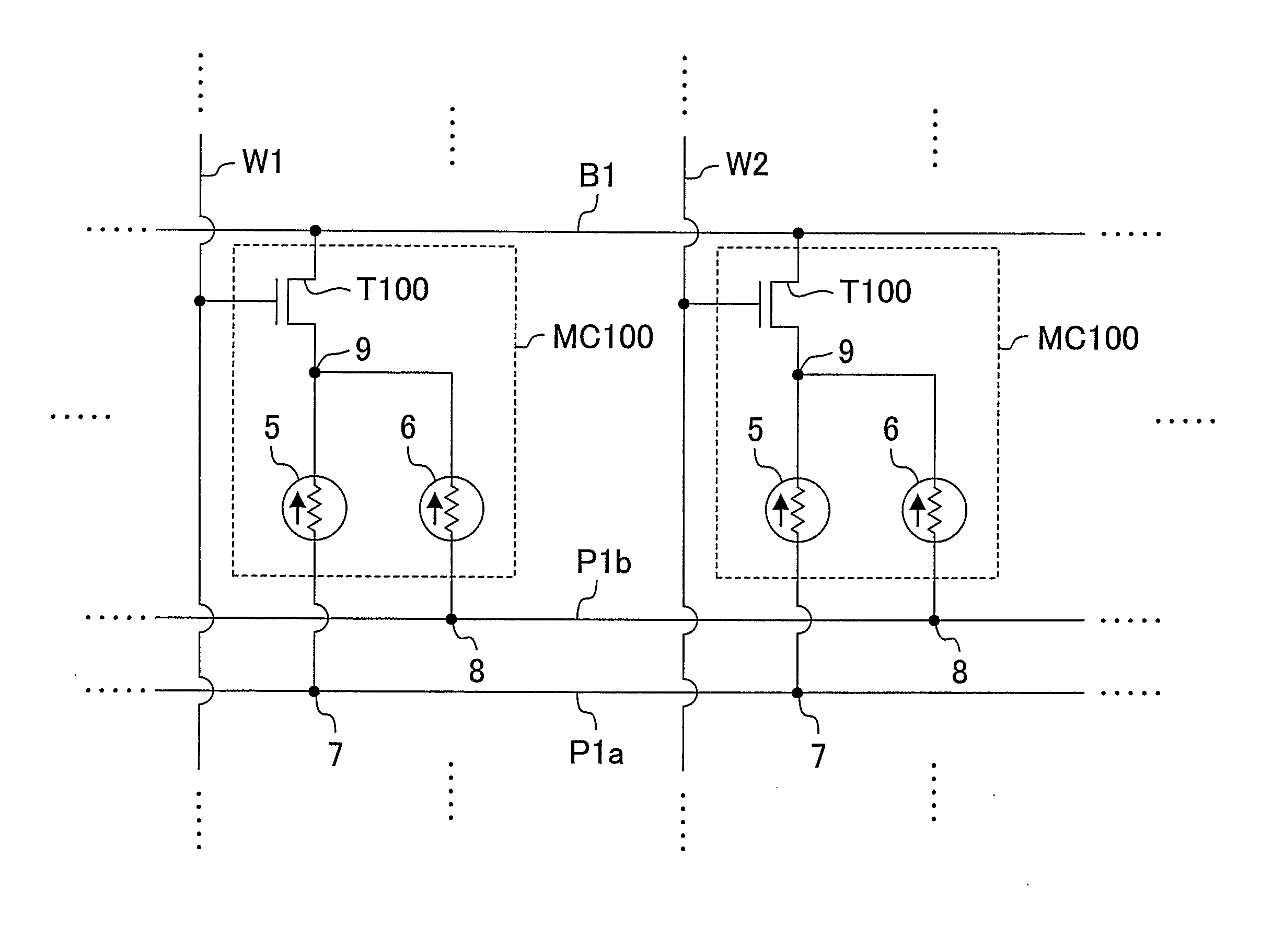
[0061] A circuit configuration of a memory array circuit according to a third embodiment is shown in FIG. 8. This memory array circuit is an example in which the memory device described in the second embodiment (FIG. 7) is incorporated in a transistor circuit. In the memory array circuit, a plurality of memory cells MC100 are arranged in rows and columns, i.e., in a matrix pattern. A plurality of word lines W1, W2, . . . are arranged in columns. A plurality of bit lines B1, . . . are arranged in rows. A plurality of plate lines P1a, P1b, . . . are also arranged in rows. Out of the plurality of memory cells MC100 included in the memory array circuit, FIG. 8 shows a portion including two memory cells MC100 associated with the word lines W1 and W2, the bit line B1 and the plate lines P1a and P1b.

[0062] Each of the memory cells MC100 includes variable resistors 5 and 6 and a transistor T100. The transistor T100 and the variable resistor 5 a...


PUM


Abstract

A first variable resistor (5) is connected between a first terminal (7) and a third terminal (9) and increases/reduces its resistance value in accordance with the polarity of a pulse voltage applied between the first terminal (7) and the third terminal (9). A second variable resistor (6) is connected between the third terminal (9) and a second terminal (8) and increases/reduces its resistance value in accordance with the polarity of a pulse voltage applied between the third terminal (9) and the second terminal (8). Given pulse voltages are applied between the first terminal (7) and the third terminal (9) and between the third terminal (9) and the second terminal (8) to reversibly change the resistance values of the first and second variable resistors (5, 6), thereby recording one bit or multiple bits of information.

Description

TECHNICAL FIELD [0001] The present invention relates to a memory device, a memory circuit and a semiconductor integrated circuit, each using a material whose resistance changes depending on an electrical pulse applied thereto. BACKGROUND [0002] With recent development of digital technology for electric equipment, requirements for nonvolatile memories have been increasing in order to store data such as images. Specifically, requirements for larger capacity of memories, reduction of power necessary for writing, higher write / read speed, longer life and others have been further increasing. At present, flash memories that achieve nonvolatility by utilizing a mechanism in which electrons are injected into a floating gate provided at the gate of a semiconductor transistor are in practical use as nonvolatile memories and are widely used as external memories for digital cameras and personal computers. [0003] However, such flash memories have many drawbacks, e.g., high write power, long write...

Claims


Application Information

Patent Timeline
IPC IPC(8): G11C17/00G11C11/56G11C13/00G11C16/02H01L27/24H01L45/00
CPCG11C11/5685G11C13/0007G11C13/003G11C13/0069G11C2013/0083G11C2213/31H01L45/147G11C2213/78G11C2213/79H01L27/2436H01L45/04H01L45/1233G11C2213/75H10B63/82H10B63/30H10B63/80H10N70/20H10N70/826H10N70/8836G11C16/00G11C11/15
Inventor MURAOKA, SHUNSAKUOSANO, KOICHITAKAHASHI, KENSHIMOTASHIRO, MASAFUMI
Owner PANASONIC CORP
Why Eureka
Try Eureka