Light emitting diode packaging structure

a technology of light-emitting diodes and packaging structures, which is applied in the direction of semiconductor devices, semiconductor/solid-state device details, electrical devices, etc., can solve the problems of reducing the output efficiency of led devices, wasting a lot of light, and reducing energy consumption, so as to increase the light output efficiency and reduce energy consumption. loss

Inactive Publication Date: 2007-07-19
EVERLIGHT ELECTRONICS
View PDF7 Cites 20 Cited by
  • Summary
  • Abstract
  • Description
  • Claims
  • Application Information

AI Technical Summary

Benefits of technology

[0009] One objective of the invention is to provide an LED packaging structure and the manuf

Problems solved by technology

Most of the light is wasted by the packaging material absorption during the multiple reflections and scatterings.
Therefo

Method used


Image

  • Light emitting diode packaging structure
  • Light emitting diode packaging structure
  • Light emitting diode packaging structure

Examples


Embodiment Construction

[0023] The present invention will be apparent from the following detailed description, which proceeds with reference to the accompanying drawings, wherein the same references relate to the same elements.

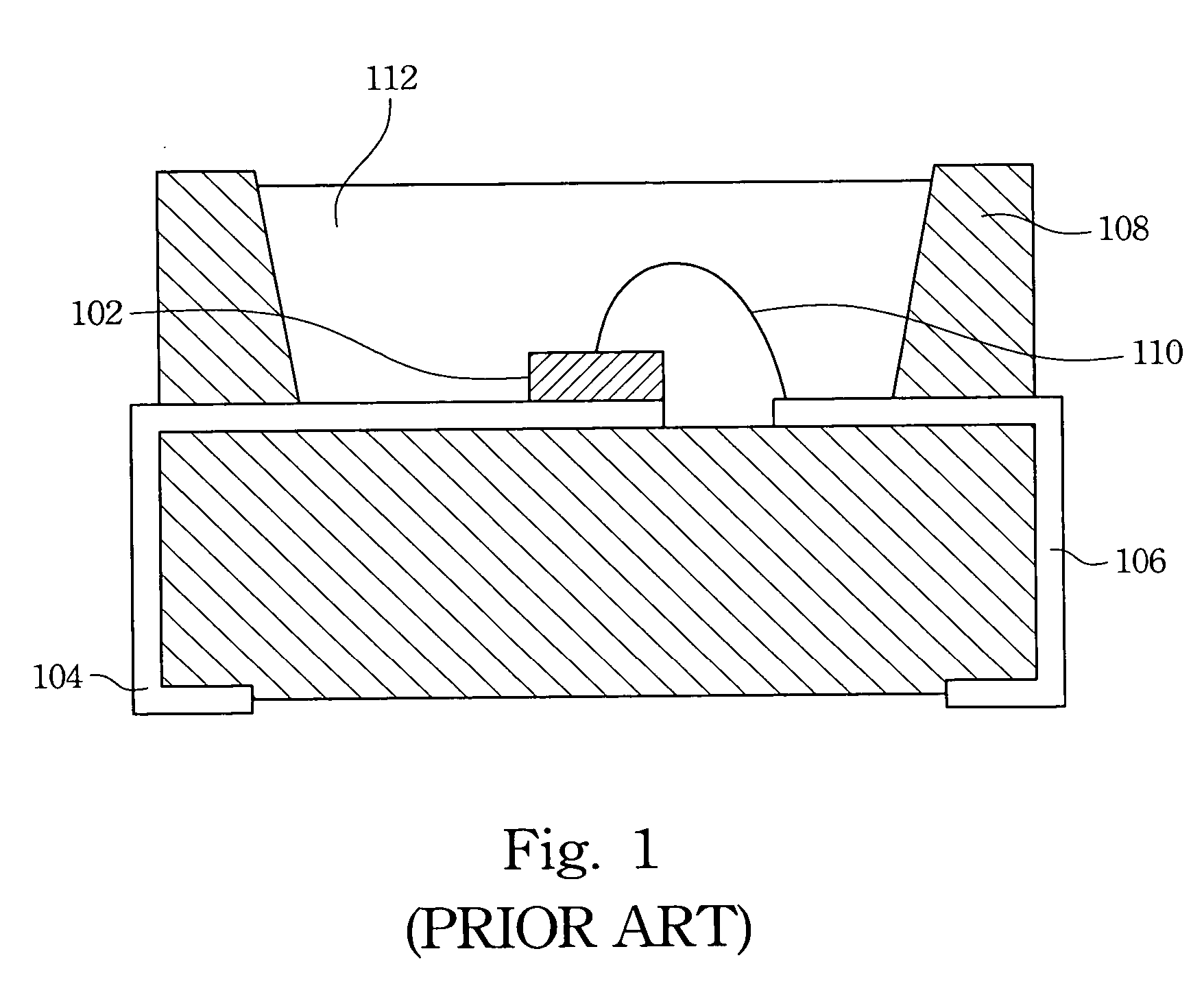
[0024] The disclosed packaging structure uses the body of the lead frame to directly form external lead pins and the reflective wall inside the chip accommodating space. The manufacturing process is simple and convenient. No additional special equipment is required. The packaging structure thus made has the advantages of reducing energy loss and increasing light output efficiency.

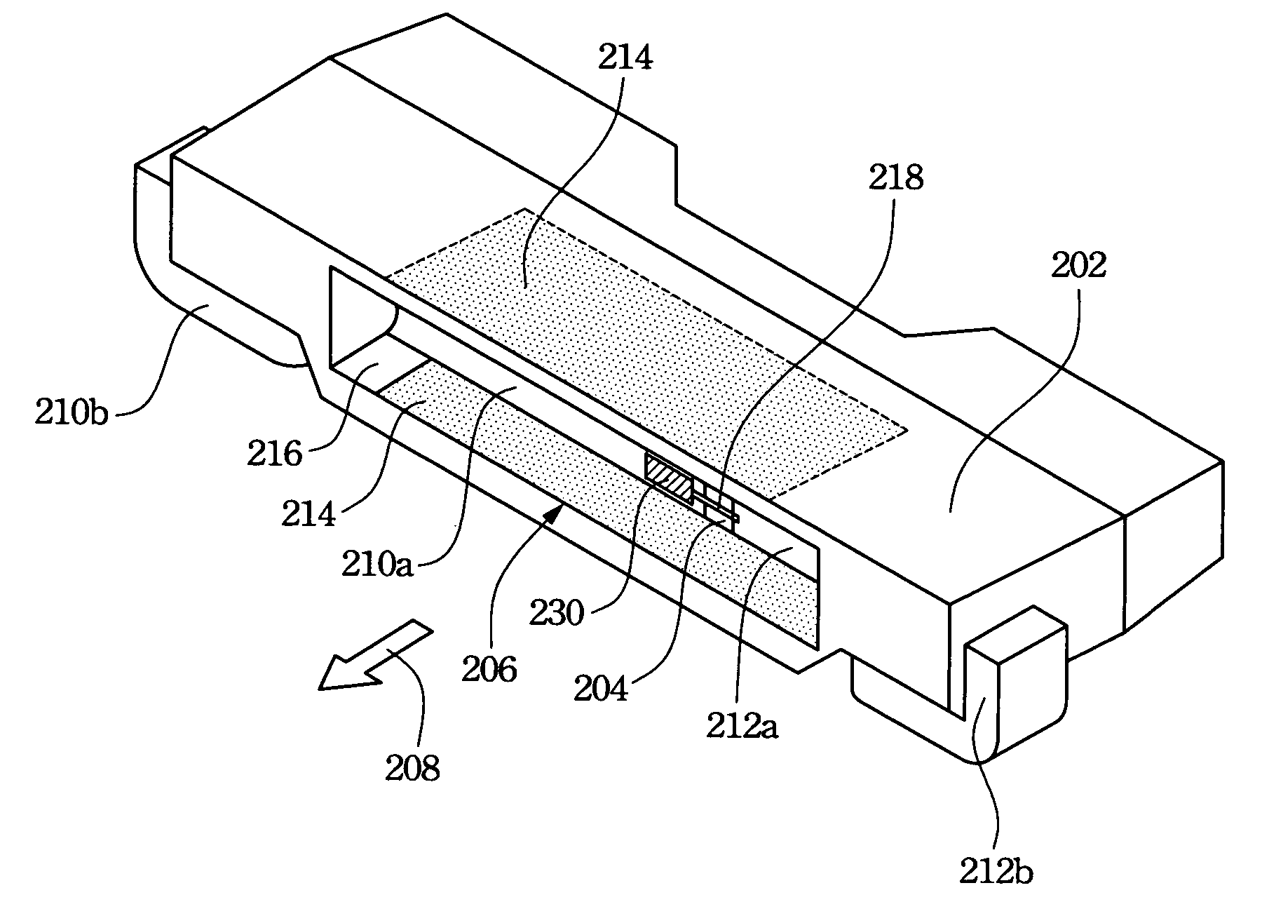
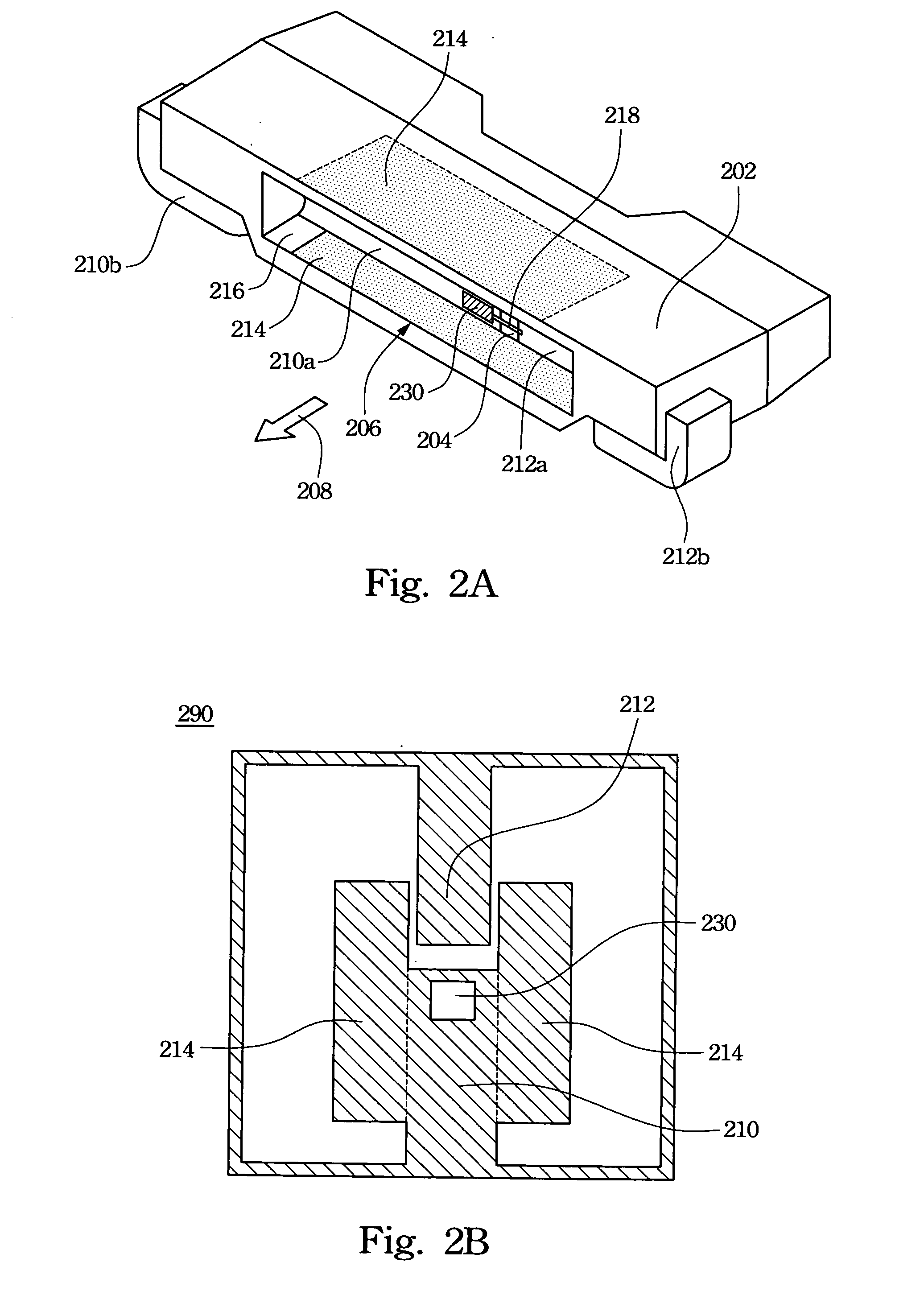
[0025] With reference to FIG. 2A, the LED packaging structure includes a packaging body 202 with a chip accommodating space 204 defined by a recession structure inside the packaging body 202 for accommodating an LED chip; a lead frame 212 whose one portion is embedded in the packaging body 202 and exposed in the chip accommodating space 204, and a reflective wall 214 connected to the lead frame 210 and ext...


PUM


Abstract

A light emitting diode (LED) packaging structure includes a package body, a lead frame and a reflective wall. The package body includes a chip accommodating space for an LED chip, and a portion of the lead frame is exposed to the chip accommodating space. The reflective wall is connected with the lead frame and extendedly bends from the lead frame to cover a sidewall of the accommodating space so that rays of the LED chip can reflect from the reflective wall mostly.

Description

RELATED APPLICATIONS [0001] The present application is based on, and claims priority from, Taiwan Application Serial Number 95102082, filed Jan. 19, 2006, the disclosure of which is hereby incorporated by reference herein in its entirety. BACKGROUND OF THE INVENTION [0002] 1. Field of Invention [0003] The invention relates to a packaging structure and the manufacturing method thereof. In particular, the invention relates to an LED packaging structure and the manufacturing method thereof. [0004] 2. Related Art [0005] Light emitting diodes (LED) have the features of long lifetime, low power consumption, safety, and fast reactions. With technical progress, the brightness of the LED becomes higher, enlarging its applications. The conventional LED is fabricated using a metal lead frame along with plastic injection molding. FIG. 1 shows a cross-sectional view of the conventional LED structure with a lead frame. [0006] Two lead frames 104, 106 are connected to the positive and negative ele...

Claims


Application Information

Patent Timeline
IPC IPC(8): H01L23/495H01L33/56H01L33/60H01L33/62H01L33/64
CPCH01L33/486H01L33/60H01L33/62H01L2224/48091H01L2224/48247H01L2924/01079H01L2924/0102H01L2924/00014H01L2924/01068
Inventor YEH, ROBERTCHUANG, SHIH-JEN
Owner EVERLIGHT ELECTRONICS
Why Eureka
Try Eureka