

Method and apparatus of fabricating semiconductor device
a technology of semiconductor devices and insulating films, which is applied in the direction of semiconductor devices, electrical equipment, basic electric elements, etc., can solve the problems of insufficient level of control of the thickness and characteristics of gate insulating films, and achieve the effect of increasing the amount of nitrogen introduction and accelerating the diffusion of nitrogen
Active Publication Date: 2007-07-19
FUJITSU LTD
View PDF12 Cites 37 Cited by
- Summary
- Abstract
- Description
- Claims
- Application Information
AI Technical Summary
Benefits of technology
[0027] In other words, even when the plasma nitriding chamber was conditioned at room temperature so as to control energy of the generated active nitrogen, reactivity between the active nitrogen and the silicon oxide film would become unnecessarily large, under high temperature of the substrate having the silicon oxide film reactive with the active nitrogen formed thereon. It is supposed that this consequently incr
Problems solved by technology
However, this method may sometimes result in only an insufficient level of control of the thickness and
Method used
View moreImage
Smart ImageViewing Examples

Examples
 PUM
 Abstract
An underlying film forming section forming an underlying film on a semiconductor substrate is provided to an apparatus of fabricating a semiconductor device. The apparatus is further provided with a cooling section cooling the semiconductor substrate and a plasma nitriding section introducing active nitrogen into the underlying film while keeping the temperature of the semiconductor substrate cooled by the cooling section at 100° C. or below. The semiconductor substrate is cooled by using liquid nitrogen or liquid helium, and by cooling a stage on which the semiconductor substrate is placed.
Description
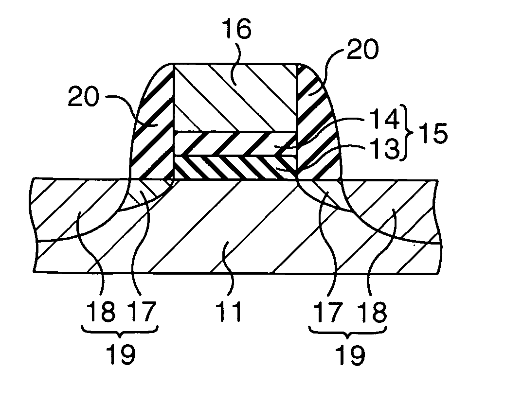
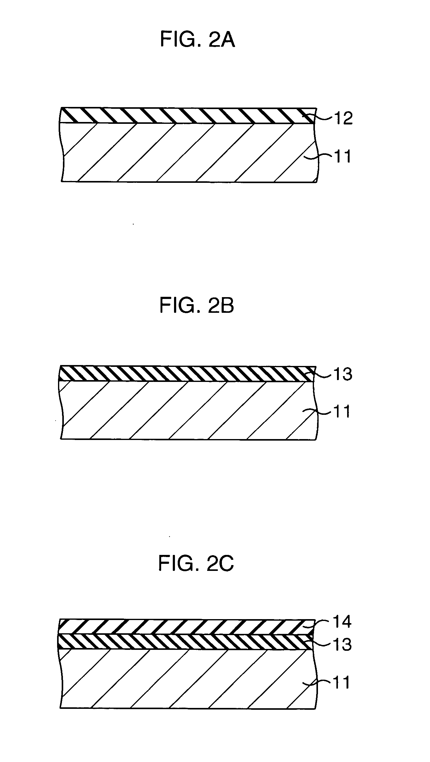
CROSS-REFERENCE TO RELATED APPLICATIONS [0001] This application is based upon and claims the benefit of priority from the prior Japanese Patent Application No. 2006-011603, filed on Jan. 19, 2006, the entire contents of which are incorporated herein by reference. BACKGROUND OF THE INVENTION [0002] 1. Field of the Invention [0003] The present invention relates to a method and an apparatus suitable for fabricating a semiconductor device capable of high-speed operation. [0004] 2. Description of the Related Art [0005] In pursuit of improvement in degree of integration and in operation speed of semiconductor integrated circuit devices, a MOSFET as a constituent thereof is becoming downsized, and a gate insulating film is becoming thinned. A gate electrode formed on the insulating film is composed solely of a polysilicon layer, or a stack of a polysilicon layer and a silicide layer. The polysilicon layer is doped with an impurity ion species at the same time as ion-implantation for source...
Claims
Login to View More Application Information
Patent Timeline
 IPC IPC(8): H01L21/84
CPCH01L21/28202H01L21/3145H01L29/517H01L29/513H01L21/823462Y10S438/908Y10S438/907H01L21/02318H01L21/02164
InventorHORI, MITSUAKI
OwnerFUJITSU LTD