Method for manufacturing silicon carbide semiconductor device

a semiconductor device and silicon carbide technology, applied in the direction of single crystal growth, polycrystalline material growth, chemistry apparatus and processes, etc., can solve the problems of reducing affecting and taking considerable time to grow the sic epitaxial films, etc., to achieve suppress the growth rate and reduce the growth rate of silicon carbide semiconductor films. , the effect of high ra

Inactive Publication Date: 2014-03-06
FUJI ELECTRIC CO LTD
View PDF0 Cites 0 Cited by
  • Summary
  • Abstract
  • Description
  • Claims
  • Application Information

AI Technical Summary

Benefits of technology

[0018]According to the aforementioned configuration, a gas atmosphere is formed in such a manner that a suitable amount of gas containing chlorine is added to raw material gas including gas containing silicon and gas containing carbon so that the introduction amount of the raw material gas contributing to the growth of the silicon carbide semiconductor film can be increased. In addition, according to the aforementioned configuration, the number of chlorine atoms in the gas containing chlorine is reduced gradually with the passage of the film formation time of the silicon carbide semiconductor film so that the nu

Problems solved by technology

However, in prior epitaxial growth methods the growth rate is low to be about several μm/h.
To grow an epitaxial film with a thickness (film thickness) of several tens or more

Method used


Image

  • Method for manufacturing silicon carbide semiconductor device
  • Method for manufacturing silicon carbide semiconductor device
  • Method for manufacturing silicon carbide semiconductor device

Examples


embodiment

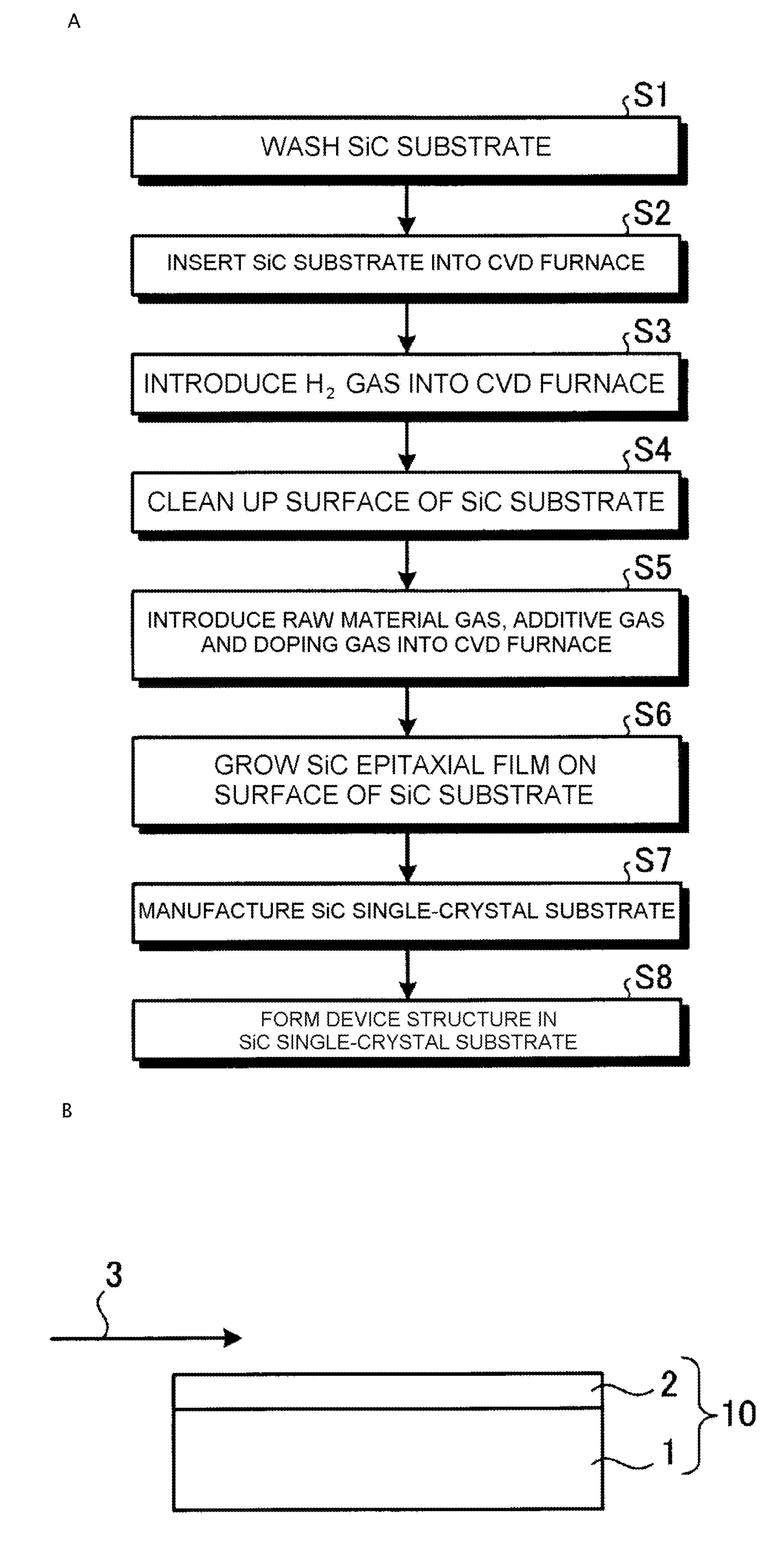
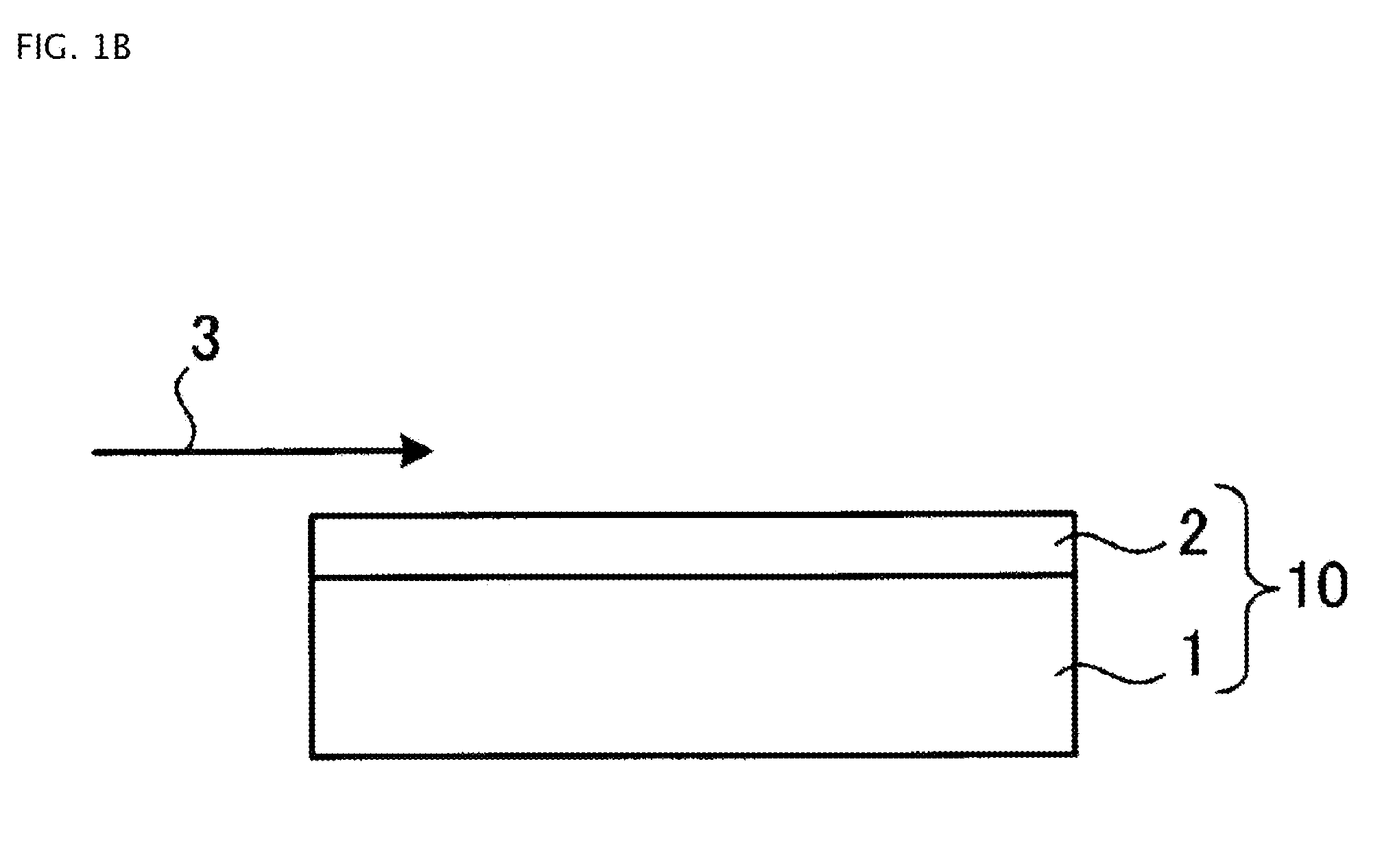
[0028]A method for manufacturing a silicon carbide semiconductor device according to an embodiment will be described in the case where a semiconductor device is produced (manufactured) using four-layered hexagonal silicon carbide (4H—SiC) as a semiconductor material, by way of example. FIG. 1A is a flow chart showing the outline of the method for manufacturing the silicon carbide semiconductor device according to the embodiment. FIG. 1B is a sectional view showing a state in which the silicon carbide semiconductor device is being manufactured according to the embodiment. First, a substrate (4H—SiC substrate) 1 made of 4H—SiC is prepared, and washed by a general organic cleaning method or a general RCA cleaning method (Step S1).

[0029]Next, 4H—SiC substrate 1 is inserted into a reacting furnace (chamber, not shown) in order to grow 4H—SiC single-crystal film (hereinafter referred to as “SiC epitaxial film (silicon carbide semiconductor film)”) 2 by a chemical vapor deposition (CVD) me...


PUM


Abstract

Gas containing Si, gas containing C and gas containing Cl are introduced into a reacting furnace. SiC epitaxial film is grown on the surface of a 4H—SiC substrate by CVD in a gas atmosphere including raw material gas, additive gas, doping gas and carrier gas. The amount of the gas containing Cl relative to the gas containing Si in the gas atmosphere is reduced gradually. At the start of growth, the number of Cl atoms in the gas containing Cl is three times as large as the number of Si atoms in the gas containing Si. The number of Cl atoms in the gas containing Cl relative to the number of Si atoms in the gas containing Si in the gas atmosphere is reduced at a rate of 0.5%/min to 1.0%/min. The method grows silicon carbide semiconductor film at a high rate.

Description

BACKGROUND OF THE INVENTION[0001]A. Field of the Invention[0002]The present invention relates to a method for manufacturing a silicon carbide semiconductor device.[0003]B. Description of the Related Art[0004]Compound semiconductors using four-layered hexagonal silicon carbide (4H—SiC) as a semiconductor material are known. When a power semiconductor device is manufactured using 4H—SiC as a semiconductor material, a 4H—SiC single-crystal film (hereinafter referred to as “SiC epitaxial film”) is epitaxially grown on a semiconductor substrate made of 4H—SiC (hereinafter referred to as “4H—SiC substrate”) so as to manufacture a SiC single-crystal substrate. ACVD (Chemical Vapor Deposition) method has been used as an epitaxial growth method.[0005]In the epitaxial growth using the CVD method, raw material gas flowing into a reaction vessel (chamber) is thermally decomposed in carrier gas, and silicon (Si) atoms are then deposited continuously on the crystal lattice of a 4H—SiC substrate s...

Claims


Application Information

Patent Timeline
IPC IPC(8): H01L21/02
CPCH01L21/02529H01L21/02378H01L21/0262C30B25/02C30B29/36H01L21/205H01L21/20
Inventor KAWADA, YASUYUKIYONEZAWA, YOSHIYUKI
Owner FUJI ELECTRIC CO LTD
Why Eureka
Try Eureka