Semiconductor device with elevated source/drain structure and its manufacture method

a semiconductor and source/drain technology, applied in the direction of semiconductor devices, electrical devices, transistors, etc., can solve the problems of inconvenient mass production, slow growth speed of semiconductor films, increased junction leak current, etc., to prevent aggregation of metal silicides, reduce lateral diffusion of impurities, and increase growth speed

Inactive Publication Date: 2005-06-09
FUJITSU LTD
View PDF1 Cites 26 Cited by
  • Summary
  • Abstract
  • Description
  • Claims
  • Application Information

AI Technical Summary

Benefits of technology

[0013] An object of this invention is to provide a semiconductor device having an elevated source / drain structure capable of mitigating the short channel effects and its manufacture method.
[0015] Impurities are implanted to form impurity diffusion regions of the source and drain, by using as a mask the sidewall spacers covering partial surfaces of the first semiconductor films. It is possible to suppress an increase in the short channel effects to be caused by the lateral diffusion of impurities.
[0018] As above, after the selective epitaxial growth is performed to form an elevated source / drain structure, the extension regions of the source and drain and the source and drain regions are formed. It is therefore possible to suppress the lateral diffusion of impurities in the extension regions and source / drain regions. Since the epitaxial growth can be made at a high temperature, the growth speed can be increased. After the source and drain regions are formed, the metal suicide film is formed. Since the metal silicide film does not experience the activation heat treatment for impurities, aggregation of metal silicide can be prevented.

Problems solved by technology

If the refractory metal silicide layer is formed on the shallow source and drain regions, junction leak current increases.
Since the growth temperature cannot be made high, the growth speed of the semiconductor film is slow.
This method is not suitable for mass production.
If the heat treatment temperature is set to 600° C. or lower, the sufficient effects of removing the native oxide film cannot be expected.
The sufficient short channel suppression effects cannot therefore be expected.
Further, since the heat treatment for diffusing impurities in the extension regions is preformed after the titanium silicide layer is formed, aggregation of titanium silicide is likely to occur.
A low resistance of the gate electrode cannot therefore be expected.

Method used


Image

  • Semiconductor device with elevated source/drain structure and its manufacture method
  • Semiconductor device with elevated source/drain structure and its manufacture method
  • Semiconductor device with elevated source/drain structure and its manufacture method

Examples


Embodiment Construction

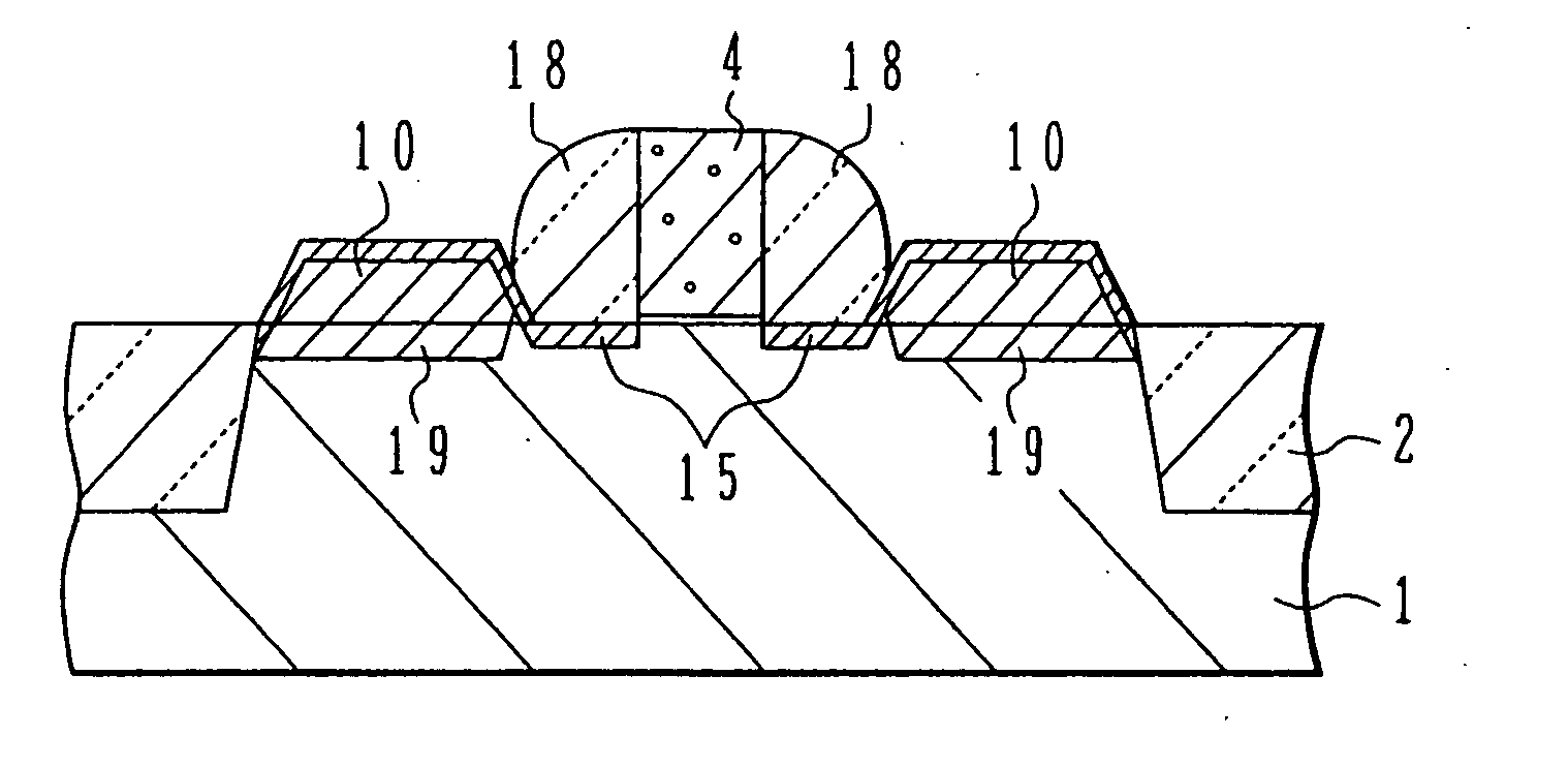
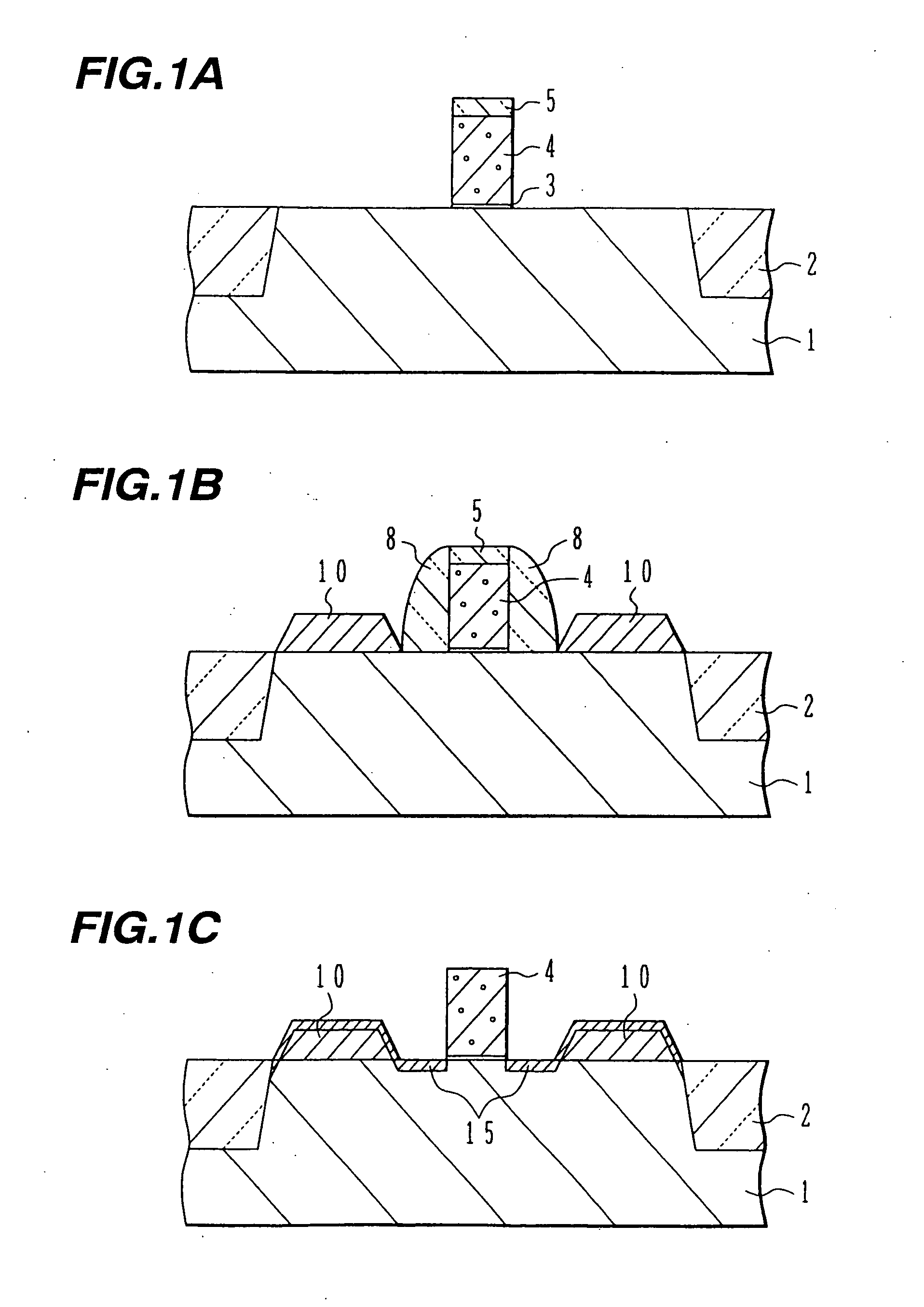
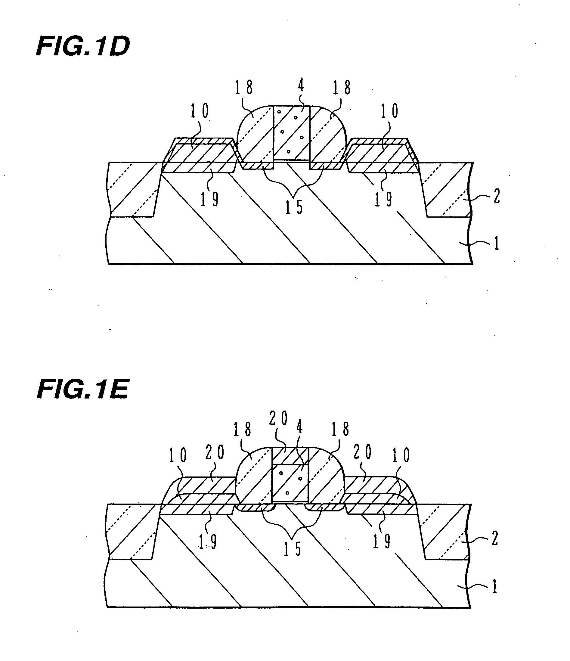
[0021] With reference to FIGS. 1A to 1E, a semiconductor device manufacture method according to an embodiment of the invention will be described.

[0022] As shown in FIG. 1A, in the surface layer of a semiconductor substrate 1 made of silicon, an element separation insulating film 2 is formed by local oxidation of silicon (LOCOS) or shallow trench isolation (STI). The element separation region 2 defines active regions. The surface of the semiconductor substrate 1 is thermally oxidized to form a silicon oxide film on the surface of each active region, the silicon oxide film having a thickness of about 2 nm and being used as a gate insulating film.

[0023] On the semiconductor substrate 1, a polysilicon film having a thickness of 70 to 120 nm is formed by chemical vapor deposition (CVD). Instead of the polysilicon film, an amorphous silicon film may be formed. A silicon nitride film having a thickness of 20 to 40 nm is formed on the polysilicon film by CVD. By covering the region where ...


PUM


Abstract

A gate electrode is formed over a partial surface area of a semiconductor substrate, with a gate insulating film being interposed therebetween. A first semiconductor film is formed over the semiconductor substrate on both sides of the gate electrode, the first semiconductor film being spaced apart from the gate electrode. An impurity diffusion region is formed in each of the first semiconductor films. An extension region is formed in the surface layer of the semiconductor substrate on both sides of the gate electrode. The extension region is doped with impurities of the same conductivity type as the impurity diffusion region and being connected to a corresponding one of the impurity diffusion regions. Sidewall spacers are formed on the sidewalls of the gate electrode, the sidewall spacers extending beyond edges of the first semiconductor films on the gate electrode side and covering partial surfaces of the first semiconductor films.

Description

CROSS REFERENCE TO RELATED APPLICATION [0001] This application is based on and claims priority of Japanese Patent Application No. 2002-251268 filed on Aug. 29, 2002, the entire contents of which are incorporated herein by reference. BACKGROUND OF THE INVENTION [0002] A) Field of the Invention [0003] The present invention relates to a semiconductor device and its manufacture method, and more particularly to a MOS semiconductor device having an elevated source / drain structure and its manufacture method. [0004] B) Description of the Related Art [0005] High speed operation and high integration of semiconductor devices require a shortened gate length and a reduced parasitic capacitance. In order to suppress the short channel effects, it is necessary to shallow source and drain regions. In order to suppress an increase in a sheet resistance to be caused by shallow source and drain regions, techniques of forming a refractory metal silicide layer on the source and drain regions are adopted....

Claims


Application Information

Patent Timeline
Patent Type & Authority Applications(United States)
IPC IPC(8): H01L21/336H01L29/78H01L21/28
CPCH01L29/66492H01L29/665H01L29/7834H01L29/6659H01L29/66628H01L29/6653H01L21/18
Inventor MORI, TOSHIFUMI
Owner FUJITSU LTD
Why Eureka
Try Eureka