Eureka AIR delivers breakthrough ideas for toughest innovation challenges, trusted by R&D personnel around the world.

Evaluation method of probe mark of probe needle of probe card

Inactive Publication Date: 2007-07-26
SOCIONEXT INC
View PDF4 Cites 12 Cited by
  • Summary
  • Abstract
  • Description
  • Claims
  • Application Information

AI Technical Summary

Benefits of technology

[0014] Another and more specific object of the present invention may be to provide an evaluation method of a probe mark of a probe needle of a probe card whereby the probe mark of the probe needle of the probe card can be easily evaluated with a high precision at low cost without manufacturing a product wafer.
[0021] According to an embodiment of the present invention, it is possible to provide the evaluation method of the probe mark of the probe needle of the probe card whereby the probe mark of the probe needle of the probe card can be easily evaluated with a high precision at low cost without manufacturing the product wafer.

Problems solved by technology

In the meantime, as the semiconductor devices have become minute recently, the pitch between the electrode pads and the size of the electrode pads have become narrower.
Therefore, in a case where the probing test is implemented for the product wafer, if the arrangement of the electrode pad is newly designed, high cost is incurred for the inspection.
In addition, if a bad situation exists in the product wafer, the probing test cannot be implemented at that time and this causes delay of product delivery to a customer.
However, these checks are not sufficient for the inspection, and therefore confirmation using the product wafer is eventually required.

Method used


Image

  • Evaluation method of probe mark of probe needle of probe card
  • Evaluation method of probe mark of probe needle of probe card
  • Evaluation method of probe mark of probe needle of probe card

Examples


Embodiment Construction

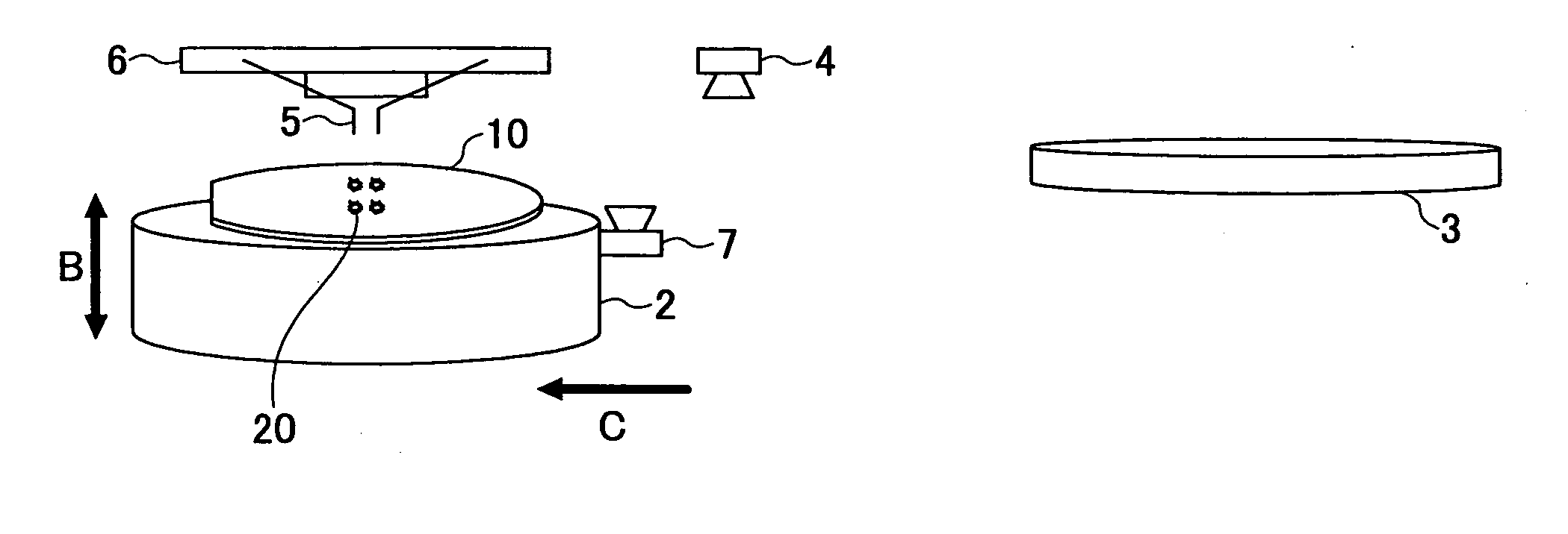
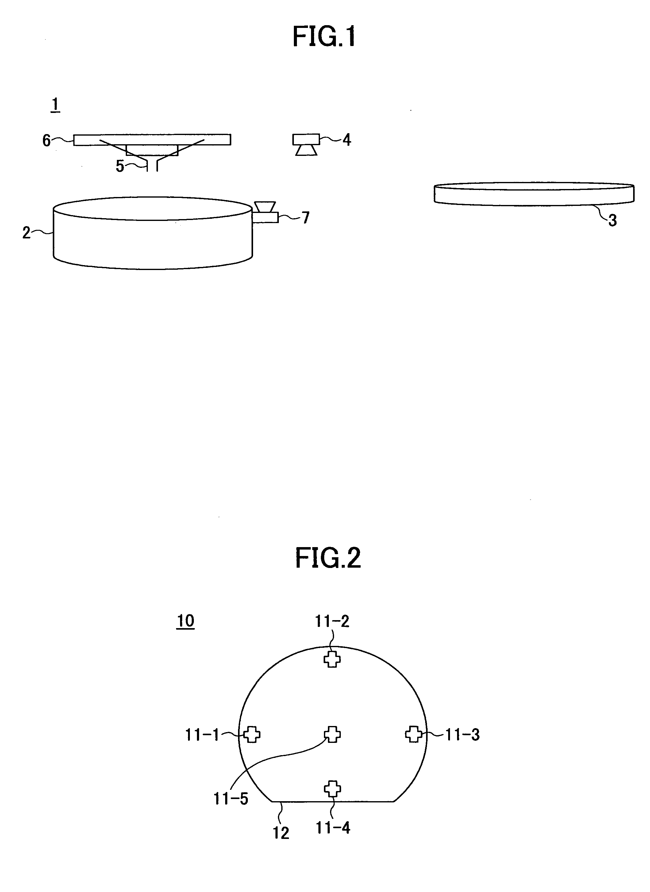
[0035] A description is given below, with reference to the FIG. 1 through FIG. 12 of embodiments of the present invention.

[0036] First, the structure of a probe device of an embodiment of the present invention is discussed with reference to FIG. 1.

[0037] Here, FIG. 1 is a schematic view showing the structure of a probe device of an embodiment of the present invention. In FIG. 1, for easily explaining processes of an evaluation method of probing of the embodiment of the present invention, illustration of a structural element not related to the process of a probe device is omitted.

[0038] Referring to FIG. 1, a probe device 1 of the embodiment of the present invention includes a wafer measuring stage (wafer mounting table) 2, a wafer carrying table 3, a wafer alignment camera 4, a probe card 6, a probe needle recognizing camera 7, and others.

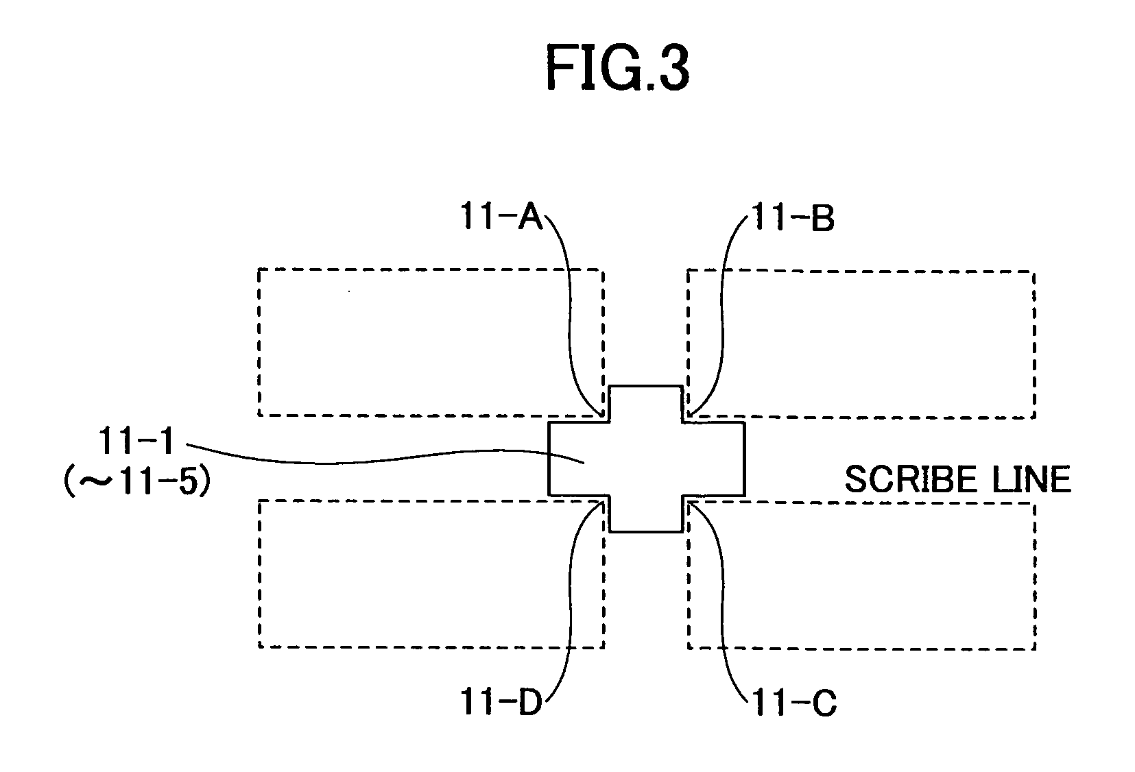
[0039] A probe mark evaluation wafer 10 (See FIG. 2) is mounted on the wafer measuring stage (wafer mounting table) 2. The wafer carrying tabl...


PUM


Abstract

An evaluation method of a probe mark of a probe needle of a probe card, includes the steps of: forming the probe mark of the probe needle on a probe mark evaluation wafer; recognizing the probe mark with imaging; and overlapping an imaginary electrode pad with the probe mark recognized by imaging so that the probe mark is evaluated.

Description

BACKGROUND OF THE INVENTION [0001] 1. Field of the Invention [0002] The present invention generally relates to evaluation methods of probe marks (contact marks or needle traces) of probe needles of probe cards, and more specifically, to an evaluation method of a probe mark (contact mark or needle trace) of a probe needle of a probe card used for inspecting an electrical property of a semiconductor element provided on a wafer. [0003] 2. Description of the Related Art [0004] Conventionally, in a product manufacturing process of a semiconductor device, an integrated circuit (hereinafter “IC”) mounted on a wafer has been connected to a tester and a function test for operating a circuit is implemented, so that a bad IC element is found at an early stage and thereby manufacturing cost of the semiconductor device is reduced and productivity of the semiconductor device is improved. [0005] In such a function test, a probe card is used as an IC inspection card in order to wire from the tester...

Claims


Application Information

Patent Timeline
IPC IPC(8): G01R31/02
CPCG01R31/2891
Inventor ENDOU, YOSHIHIKOARISAKA, YOSHIKAZUMIYAZAKI, TATSUYA
Owner SOCIONEXT INC
Why Eureka
Eureka Blog
Learn More