Organic light-emitting display

a light-emitting display and organic technology, applied in the direction of basic electric elements, electrical equipment, semiconductor devices, etc., can solve the problems of space occupation, increased product volume, and shrinking the volume of end products, so as to reduce space occupation and wastage

Active Publication Date: 2007-08-02
AU OPTRONICS CORP
View PDF24 Cites 9 Cited by
  • Summary
  • Abstract
  • Description
  • Claims
  • Application Information

AI Technical Summary

Benefits of technology

[0010] The organic light-emitting pixel area for displaying an image and the circuit for driving the organic light-emitting pixel area, are defined on the first substrate; the system circuitry is disposed on the second substrate which is opposite from the first substrate. Through a conductive layer raised by a pad, the first substrate is capable of electrically connecting to the second substrate. Compared to the prior art fabricating the system circuitry which comprises a CPU, a graphic controller, a voltage regulator, a timing circuit on a printed circuit board, the present invention disposes the system circuitry on the second substrate which is in non-use and is opposite from the first substrate. In this manner, the present invention does not arrange the printed circuit board, thereby reducing space occupancy and wastage.

Problems solved by technology

However, such design occupies space and increases product volume.
Although manufacturers tend to integrate systems on panel (SOP), due to a limitation on LTPS process, some circuits such as a central processing unit occupies quite a large area so that the panel can only occupy a smaller area as well.
Therefore, that is a disadvantage of shrinking a volume of the end product.

Method used


Image

  • Organic light-emitting display
  • Organic light-emitting display
  • Organic light-emitting display

Examples


first embodiment

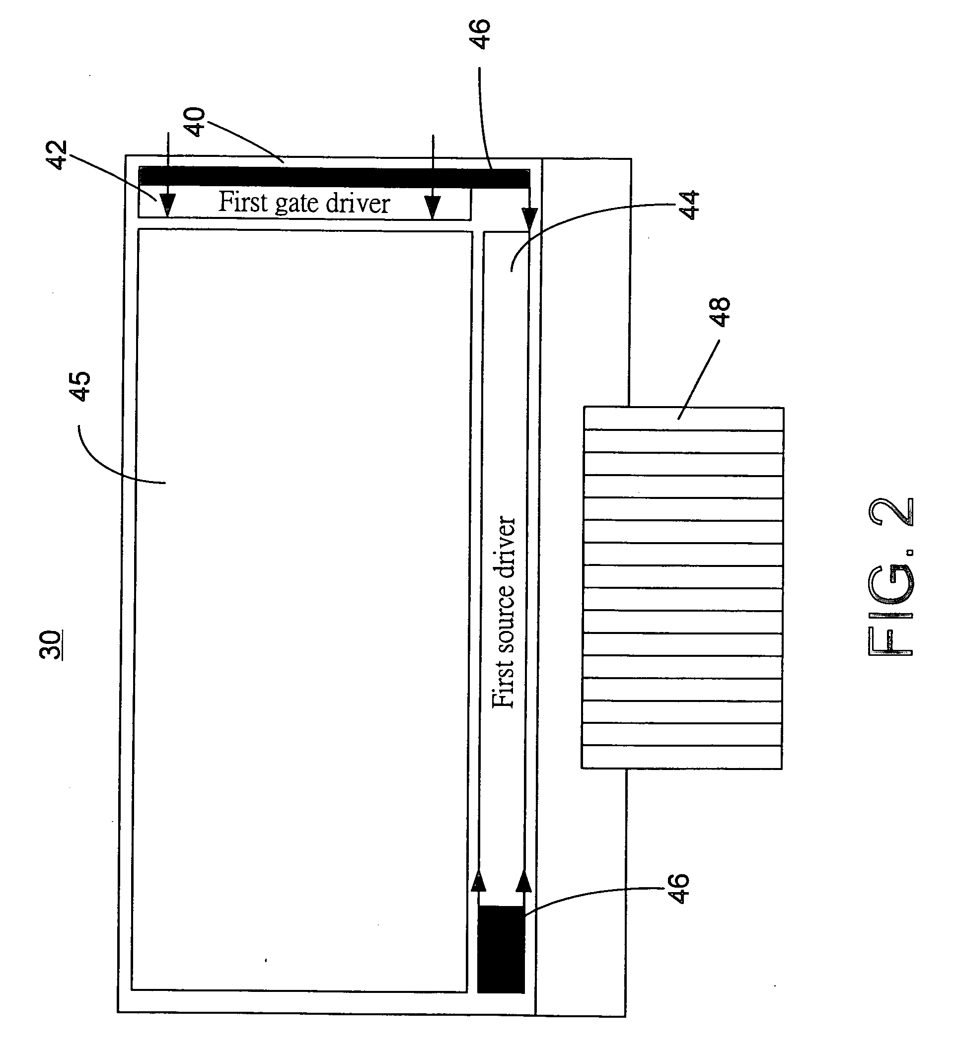
[0026]FIG. 2 is a bottom view of the organic light-emitting display according to the present invention.

[0027]FIG. 3 is a top view of the first embodiment of the organic light-emitting display according to the present invention.

[0028]FIG. 4 is a side view of the first embodiment of the organic light-emitting display according to the present invention.

[0029]FIGS. 5A, 5B, and 5C depict various connections of the first substrate and the second substrate by means of the conductive member according to the present invention.

second embodiment

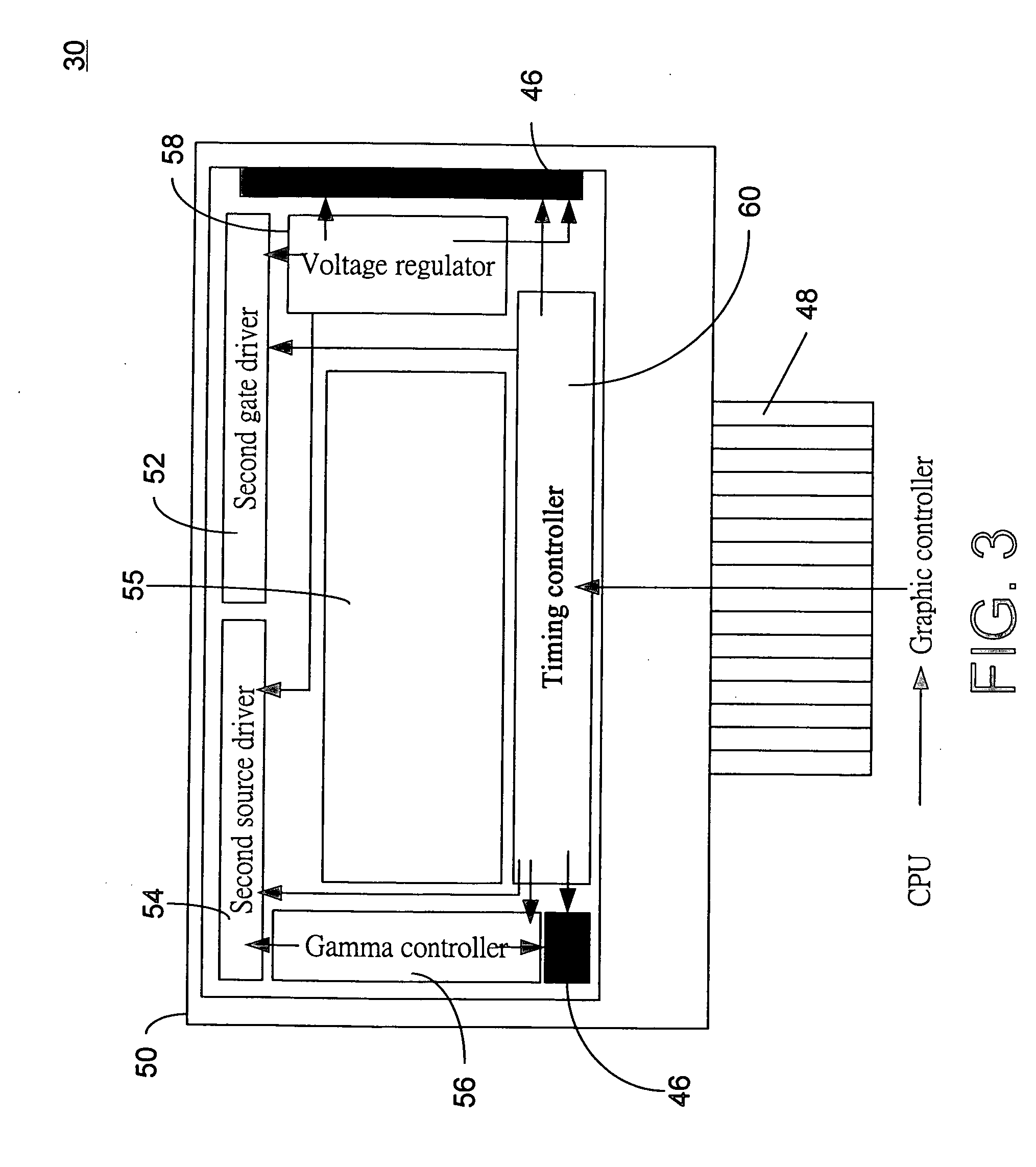
[0030]FIG. 6 is a bottom view of the organic light-emitting display according to the present invention.

[0031]FIG. 7 is a top view of the second embodiment of the organic light-emitting display according to the present invention.

[0032]FIG. 8 is a side view of the second embodiment of the organic light-emitting display according to the present invention.


PUM


Abstract

An organic light-emitting display (OLED) includes a first substrate, a first organic light-emitting pixel area, a first driver, a second substrate, a system circuitry, and a conductive member. The second substrate is opposite to the first substrate. The first organic light-emitting pixel area is defined on the first substrate and is sealed between the first substrate and the second substrate. The first driver disposed on the first substrate is used for driving the first organic light-emitting pixel area to generate images. The system circuitry disposed on the second substrate is for electrically connected to the first driver. The first substrate and the second substrate are electrically connected with each other through the conductive member.

Description

BACKGROUND OF THE INVENTION [0001] 1. Field of the Invention [0002] The present invention relates to an organic light-emitting display, and more particularly, to an organic light-emitting display integrating logic circuitry and an organic light-emitting pixel area on a substrate. [0003] 2. Description of the Related Art [0004] With a rapid development of monitor types, novelty and colorful monitors with high resolution, e.g., liquid crystal displays (LCDs), are indispensable components used in various electronic products such as monitors for notebook computers, personal digital assistants (PDA), digital cameras, and projectors. The demand for the novelty and colorful monitors has increased tremendously. [0005] Liquid crystal display (LCD) monitors control pixel luminance by adjusting voltage drop applied on a liquid crystal layer of the liquid crystal display. Differing from liquid crystal displays (LCDs), Organic Light Emitting Displays (OLEDs) determine the pixel luminance by adju...

Claims


Application Information

Patent Timeline
Patent Type & Authority Applications(United States)
IPC IPC(8): H01L33/00
CPCH01L25/048H01L27/3267H01L27/3288H01L27/3286H01L27/3276H01L2924/0002H10K59/90H10K59/128H10K59/176H10K59/179H10K59/131H01L2924/00
Inventor LEE, HSIN-HUNGCHANG, YI-CHENG
Owner AU OPTRONICS CORP
Why Eureka
Try Eureka