Aluminum leadframes for semiconductor QFN/SON devices

a technology of leadframes and semiconductors, applied in semiconductor devices, semiconductor/solid-state device details, electrical apparatus, etc., can solve the problems of more and more complicated to find a satisfactory solution for maintaining good adhesion, and achieve good adhesion, prevent moisture ingress and corrosion, and easy bondability

Active Publication Date: 2007-08-02
TEXAS INSTR INC
View PDF8 Cites 31 Cited by
  • Summary
  • Abstract
  • Description
  • Claims
  • Application Information

AI Technical Summary

Benefits of technology

[0013] It is a technical advantage of the present invention to provide the aluminum leadframes so that surface mount technologies based on solder for attaching lead portions (with water-soluble flux or mild fluxes not requiring rinse steps) can be continued. The end user of the semiconductor product can continue to employ the installed assembly equipment base.
[0014] It is another technical advantage to provide easy bondability under the conditions defined by fine pitch bonding.
[0015] As a further advantage, the present invention provides the aluminum leadframes so that they exhibit good adhesion to the molding compounds used in plastic packages, thus preventing moisture ingress and corrosion, and also exhibit good corrosion protection of the leads by the post-mold plating process.

Problems solved by technology

Hand in hand, however, with the scaling of package dimensions grew the technical challenges to maintain package reliability and optimize resistance against delamination, corrosion, warpage, and thermomechanical stress.
In recent years, a number of technical trends have made it more and more complicated to find a satisfactory solution for maintaining good adhesion.

Method used


Image

  • Aluminum leadframes for semiconductor QFN/SON devices
  • Aluminum leadframes for semiconductor QFN/SON devices
  • Aluminum leadframes for semiconductor QFN/SON devices

Examples


Embodiment Construction

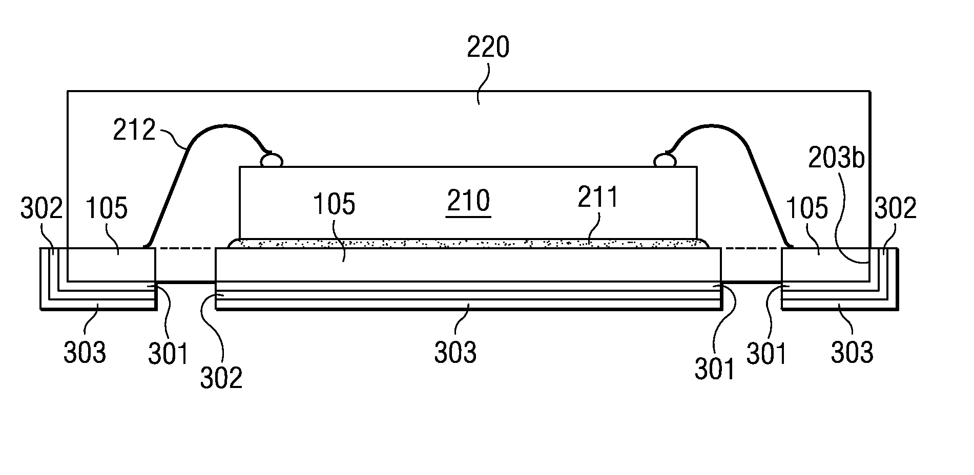
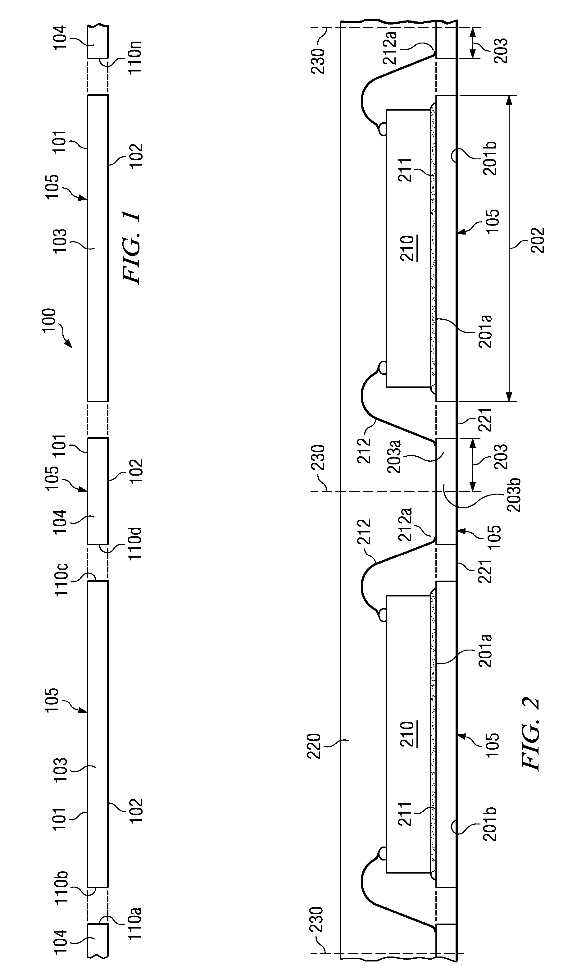
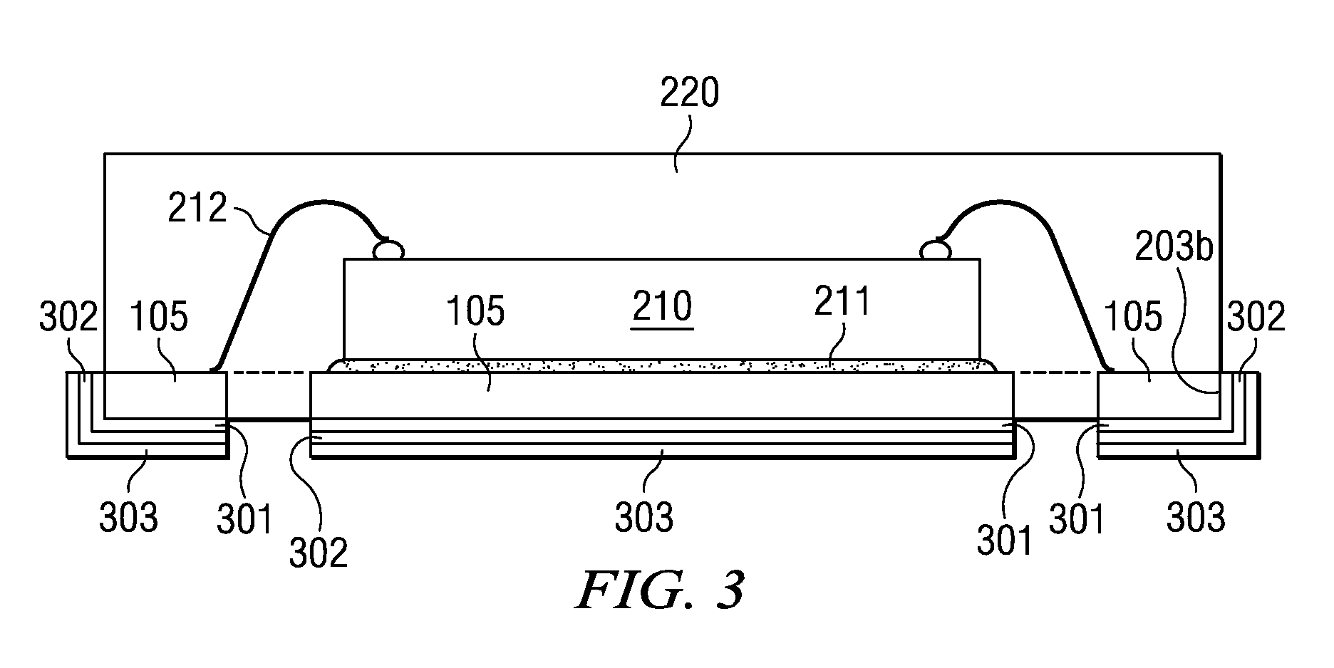
[0020] In conventional surface mount packages for semiconductor devices, which have cantilevered leads bent in a small-outline S-shape or J-shape, the leadframe material is expected to provide the ductility to offer an elongation of at least 5 to 10% in order to satisfy the requirements of outer segment forming, which is usually the last process step in the fabrication flow. The metal ductility needed for the forming process is readily provided by the ductility of copper or copper alloy as starting material. On the other hand, to provide a similar metal ductility with aluminum as starting material of the leadframe is much more challenging. Material characteristics such as thermal history, alloyed mixtures, or plated surface metal layers have to be carefully selected in order to make aluminum suitable as base material for leadframes with cantilevered leads.

[0021] Applicant recognizes that these requirements and limitations become much less of concern in leadframes, which lack cantil...


PUM


Abstract

A post-mold plated semiconductor device has an aluminum leadframe (105) with a structure including a chip mount pad and a plurality of lead segments without cantilevered lead portions. A semiconductor chip (210) is attached to the chip mount pad, and conductive connections (212) span from the chip to the aluminum of the lead segments. Polymeric encapsulation material (220), such as a molding compound, covers the chip, the connections, and portions of the aluminum lead segments without leaving cantilevered segment portions. Preferably by electroless plating, a zinc layer (301) and a nickel layer (302) are on those portions of the lead segments, which are not covered by the encapsulation material including the aluminum segment surfaces (at 203b) formed by the device singulation step, and a layer (303) of noble metal, preferably palladium, is on the nickel layer.

Description

FIELD OF THE INVENTION [0001] The present invention is related in general to the field of semiconductor devices and processes, and more specifically to the materials and fabrication of leadframes for small integrated circuit devices and semiconductor components. DESCRIPTION OF THE RELATED ART [0002] Since the introduction of the concept of Quad Flat No-Lead (QFN) and Small Outline No-Lead (SON) packages for semiconductor devices, these packages have been on a steep learning curve for miniaturization. Today, some members of these categories are favorites in semiconductor applications due to the small package size (area as well as thickness). Hand in hand, however, with the scaling of package dimensions grew the technical challenges to maintain package reliability and optimize resistance against delamination, corrosion, warpage, and thermomechanical stress. The decisive factor in these reliability efforts is the leadframe of the package. [0003] Leadframes for semiconductor devices pro...

Claims


Application Information

Patent Timeline
Patent Type & Authority Applications(United States)
IPC IPC(8): H01L23/495H01L21/00
CPCH01L21/561H01L2924/15747H01L24/45H01L24/48H01L24/97H01L2224/45014H01L2224/45124H01L2224/45144H01L2224/45147H01L2224/48091H01L2224/48247H01L2224/48465H01L2224/73265H01L2224/97H01L2924/01012H01L2924/01013H01L2924/01014H01L2924/01015H01L2924/01025H01L2924/01029H01L2924/0103H01L2924/01032H01L2924/01033H01L2924/01046H01L2924/01047H01L2924/0105H01L2924/01078H01L2924/01079H01L2924/01082H01L2924/10253H01L2924/10329H01L2924/14H01L23/49582H01L2924/15724H01L2924/01028H01L2924/01045H01L2924/01023H01L2924/01006H01L2924/01005H01L2224/32245H01L2924/00014H01L2224/85H01L2224/83H01L2924/00H01L2924/00012H01L2924/181H01L24/73H01L2924/206
Inventor ABBOTT, DONALD C.
Owner TEXAS INSTR INC
Why Eureka
Try Eureka