Nanowire heterostructures and methods of forming the same

a heterostructure and nanowire technology, applied in the field of nanowire heterostructures and methods of forming the same, can solve the problems of inability to efficiently produce such ners-active structures, and inability to manufacture ners-active structures in significant time and money

Active Publication Date: 2007-08-02
HEWLETT PACKARD DEV CO LP
View PDF12 Cites 38 Cited by
  • Summary
  • Abstract
  • Description
  • Claims
  • Application Information

AI Technical Summary

Problems solved by technology

As a result, powerful, costly laser sources typically are used to generate high intensity excitation radiation to increase the weak Raman signal for detection.
Also, the inability to efficiently produce such NERS-active structures is impeding research directed to completely understanding the enhancement mechanisms and, therefore, the ability to optimize the enhancement effect.
In addition, NERS-active structures require significant time and money to fabricate.

Method used


Image

  • Nanowire heterostructures and methods of forming the same
  • Nanowire heterostructures and methods of forming the same
  • Nanowire heterostructures and methods of forming the same

Examples


Embodiment Construction

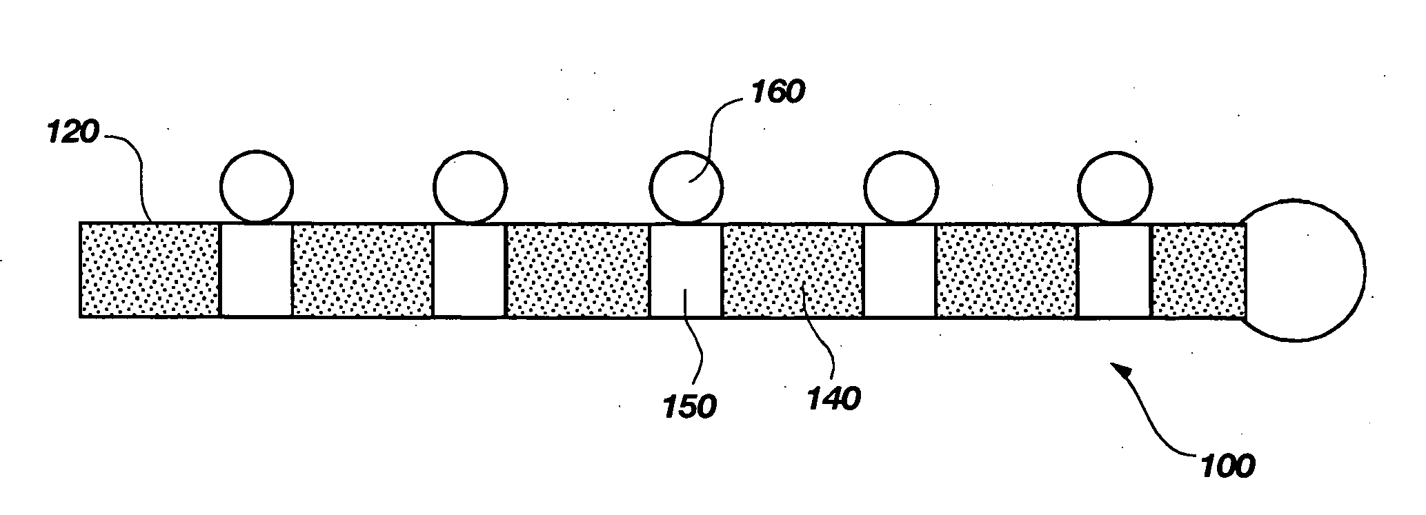
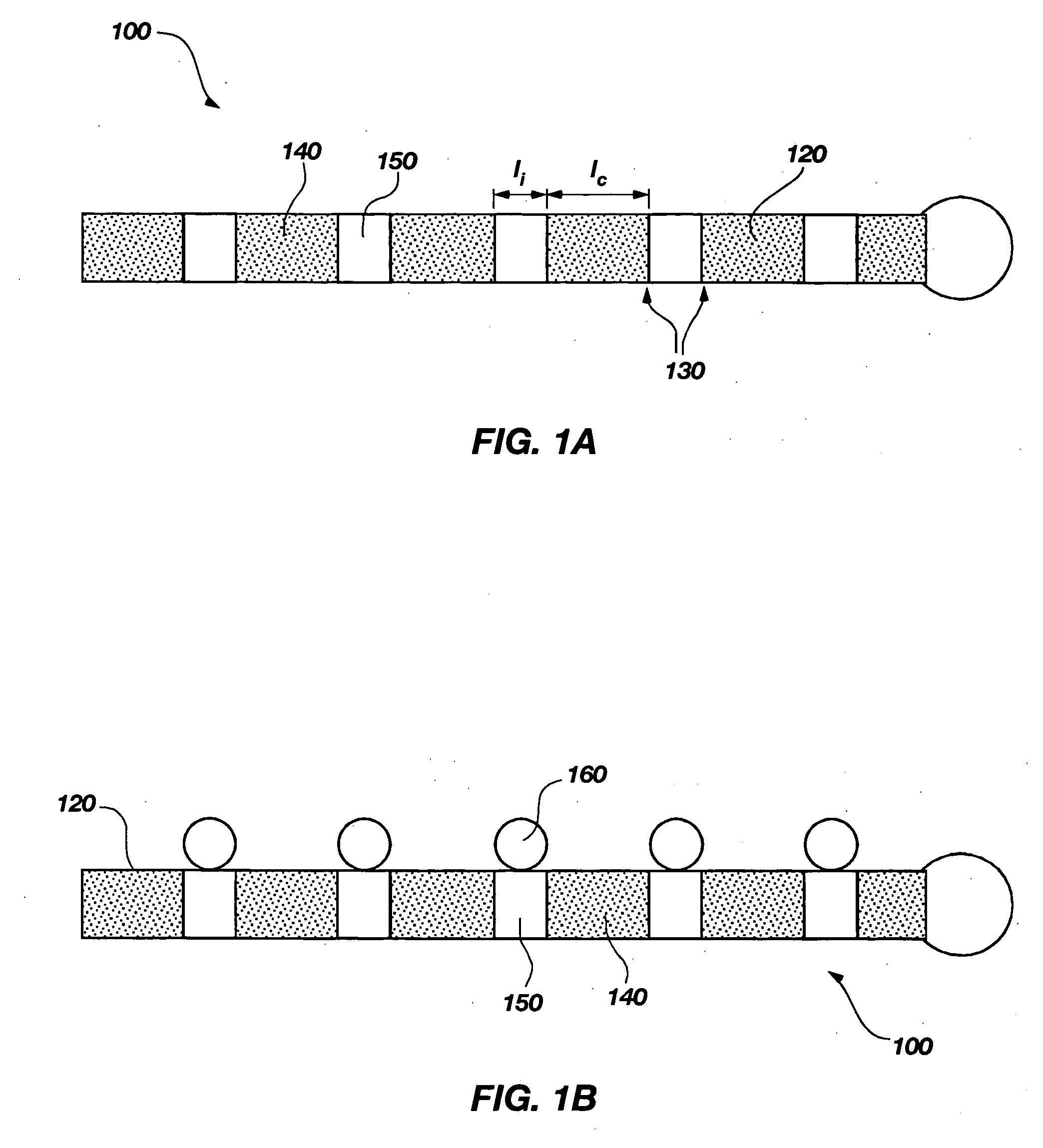
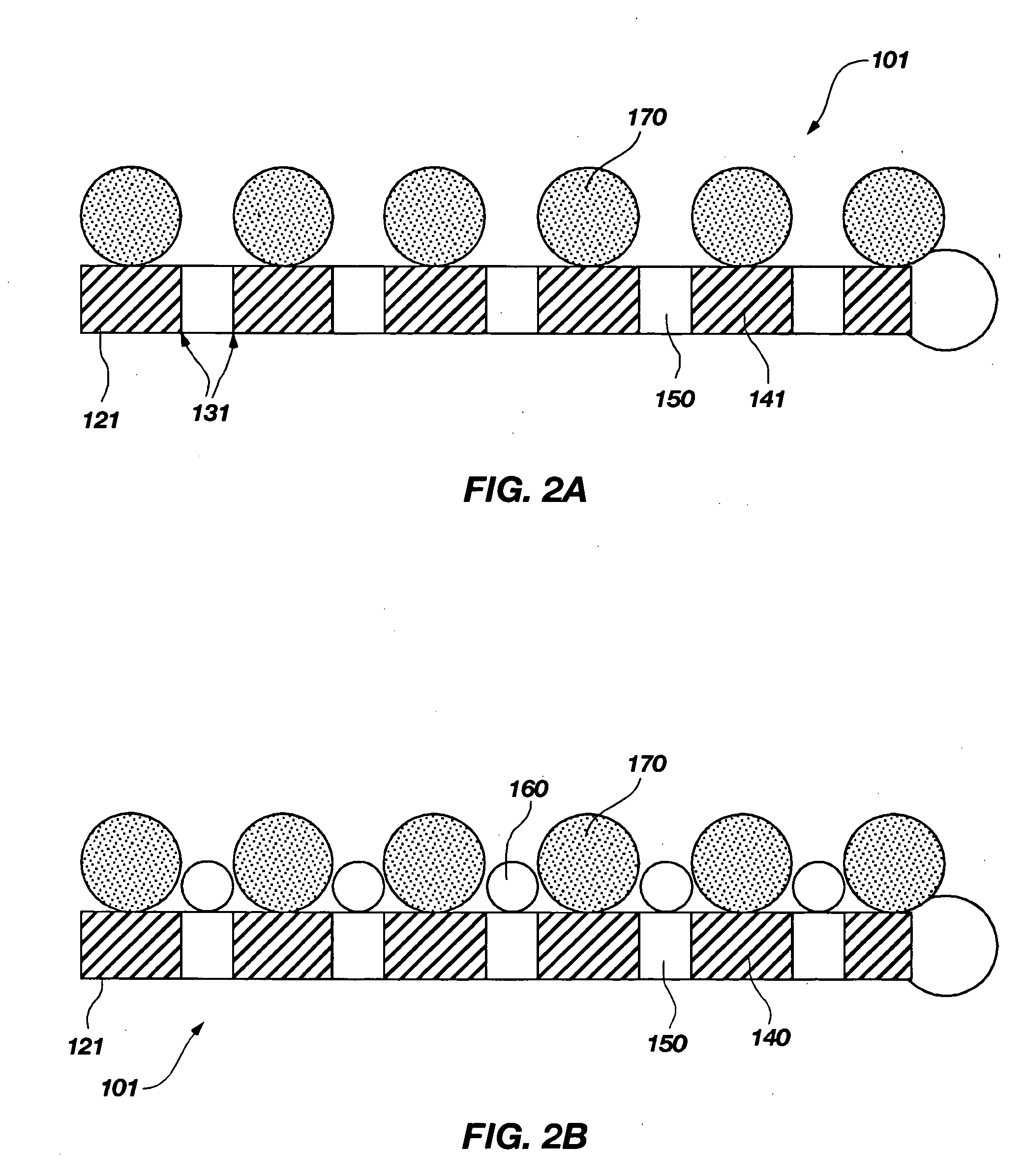
[0026] The present invention, in a number of embodiments, includes NERS-active structures including heterostructure nanowires which allow for improved enhancement of the Raman scattered signal intensity relative to conventional NERS-active structures, methods for forming NERS-active structures, NERS systems including NERS-active structures, and methods for performing NERS using such systems.

[0027] The term “NERS-active structure” as used herein means a structure that is capable of increasing the number of Raman-scattered photons that are scattered by a molecule when the molecule is located adjacent to the structure and the molecule and structure are subjected to electromagnetic radiation.

[0028] The term “NERS-active material” as used herein means a material that, when formed into appropriate geometries or configurations, is capable of increasing the number of Raman-scattered photons that are scattered by a molecule when the molecule is located adjacent the material and when the mo...


PUM

PropertyMeasurementUnit
lengthaaaaaaaaaa
lengthaaaaaaaaaa
diameteraaaaaaaaaa

Abstract

A NERS-active structure is disclosed that includes at least one heterostructure nanowire. The at least one heterostructure nanowire may include alternating segments of an NERS-inactive material and a NERS-active material in an axial direction. Alternatively, the alternating segments may be of an NERS-inactive material and a material capable of attracting nanoparticles of a NERS-active material. In yet another alternative, the heterostructure nanowire may include a core with alternating coatings of an NERS-inactive material and a NERS-active material in a radial direction. A NERS system is also disclosed that includes a NERS-active structure. Also disclosed are methods for forming a NERS-active structure and methods for performing NERS with NERS-active structures.

Description

FIELD OF THE INVENTION [0001] The invention relates to nano-enhanced Raman spectroscopy (NERS). More particularly, the invention relates to NERS-active structures including features having nanoscale dimensions, methods for forming NERS-active structures, and methods for performing NERS using NERS-active structures. BACKGROUND OF THE INVENTION [0002] Raman spectroscopy is a well-known technique for performing chemical analysis. In conventional Raman spectroscopy, high intensity monochromatic light provided by a light source, such as a laser, is directed onto an analyte (or sample) that is to be chemically analyzed. A majority of the incident photons are elastically scattered by the analyte molecule. In other words, the scattered photons have the same energy, and thus the same frequency, as the photons that were incident on the analyte. However, a small fraction of the photons (i.e., about 1 in 107 photons) are inelastically scattered by the analyte molecules. These inelastically scat...

Claims


Application Information

Patent Timeline
Patent Type & Authority Applications(United States)
IPC IPC(8): G01J3/44G01N21/65
CPCB82Y15/00G02B6/107G01N21/658B82Y20/00
Inventor KAMINS, THEODORE I.BRATKOVSKI, ALEXANDRE M.SHARMA, SHASHANK
Owner HEWLETT PACKARD DEV CO LP
Why Eureka
Try Eureka