Method for Fabricating Circuit Board with Conductive Structure

a technology of conductive structure and circuit board, which is applied in the direction of printed circuit aspects, conductive pattern formation, printed circuit components, etc., can solve the problems of low yield of stencil printing technology, circuit board with high circuit density experiences significant difficulty in allocation and adhesion, and achieves low connectivity. high

Inactive Publication Date: 2007-08-16
PHOENIX PRECISION TECH CORP
View PDF3 Cites 23 Cited by
  • Summary
  • Abstract
  • Description
  • Claims
  • Application Information

AI Technical Summary

Benefits of technology

[0022]The first and second electrically connecting structures are formed on the first and second electrically connecting pads from different materials. The first electrically connecting structure consists of electrically connecting solder material, and is formed by electroplating; while the second electrically connecting structure consists of pre-solder bumps formed of tin, silver, gold, bismuth, lead, zinc, copper or other compound metals, such bumps being formed by stencil printing. The first electricall

Problems solved by technology

However, a portion of the electrically connecting pads is covered by an insulating protective layer covering the electrically connecting pads, which causes the size of the exposed electrically connecting pads to be smaller.
In addition, This lack of exposure causes a problem in allocating the subsequent solder material, causing the solder to be poorly adhered on the electrically connecting pads, resulting in low yield of such stencil printing technology.
In particul

Method used


Image

  • Method for Fabricating Circuit Board with Conductive Structure
  • Method for Fabricating Circuit Board with Conductive Structure
  • Method for Fabricating Circuit Board with Conductive Structure

Examples


first embodiment

The First Embodiment

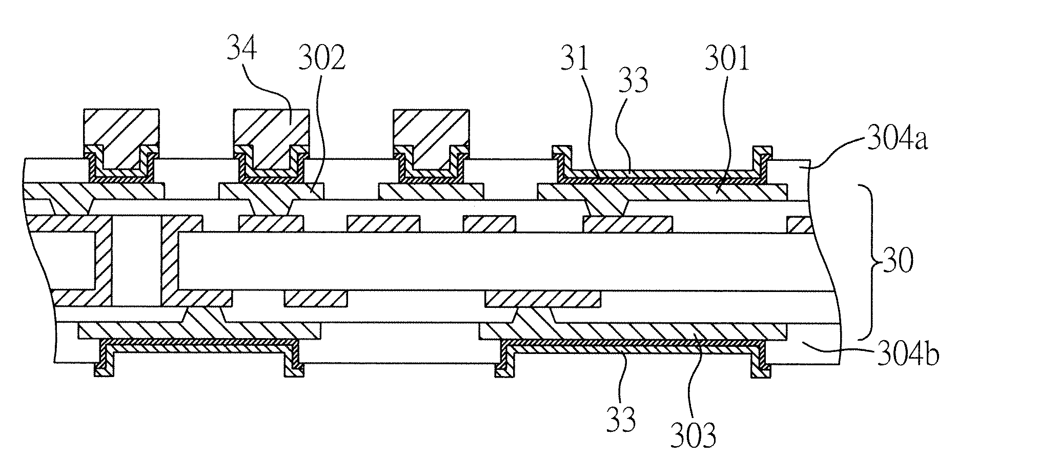
[0054]Referring to FIGS. 3A to 3F, cross-sectional views are depicted of a proposal for a method for fabricating a circuit board with an electrically connecting structure. Note that all the drawings are simplified and only the basic construction of the present invention is shown. Therefore, elements appearing in the figures for the present invention are not drawn as to real numbers, shapes, and sizes as used in actual practice. The numbers, shapes and sizes are variable design matters, and the arrangements of the elements can be more complicated.

[0055]First of all, referring to FIG. 3A, a circuit board 30 is provided with a first surface 30a and a second surface 30b, and the first surface 30a has a plurality of differently sized first electrically connecting pads 301 and second electrically connecting pads 302, while the second surface 30b has a plurality of third electrically connecting pads 303. Additionally, first and second insulating protective layers 304a, ...

second embodiment

The Second Embodiment

[0065]Referring to FIGS. 4A to 4F, another fabricating method is provided for the present invention. The main difference from the foregoing embodiment is that the first and second electrically connecting structures are formed respectively on the surfaces and in the openings of the first and second insulating protective layer. Then, the second electrically connecting structures are formed by the stencil printing on the first conductive layer of the surface of the second electrically connecting pads. The detailed description is as followings.

[0066]Firstly, referring to FIG. 4A, a circuit board 30 is provided with a first surface 30a and a second surface 30b, and the first surface 30a has a plurality of first electrically connecting pads 301 and a second electrically connecting pads 302, while the second surface 30b has a plurality of third electrically connecting pads 303. Moreover, first and second insulating protective layers 304a, 304b are formed on the first a...

third embodiment

The Third Embodiment

[0073]Referring to FIGS. 5A to 5D, yet another fabricating method for the present invention is depicted. The difference from the foregoing embodiment is that the first and second resist layers are formed on the first and second conductive layers by laminating. The detailed descriptions are as followings.

[0074]Firstly, referring to FIG. 5A, first and second conductive layers 31a, 31b are formed on the surface of the first and second insulating protective layers 304a, 304b and in the openings 305a, 305b of the first and second insulating protective layers 304a, 304b on the circuit board 30. The first and second conductive layers 31a, 31b are electrically connected to the first, second, and third electrically connecting pads 301, 302, 303. Then, first and second resist layers 32a, 32b are formed on the first and second conductive layers 31a, 31b by laminating.

[0075]Secondly, referring to FIG. 5B, a plurality of openings 321a, 321b corresponding to the first and thir...


PUM

PropertyMeasurementUnit
Electrical conductoraaaaaaaaaa

Abstract

A method for fabricating a circuit board having a conductive structure is disclosed. The method includes: forming first and second insulating protective layers respectively on first and second surfaces of a circuit board; forming a conductive layer on the first insulating protective layer and the openings; forming first and second resist layers on the conductive layer and the second insulating protective layer respectively; forming first electrically connecting structures by electroplating on the exposed conductive layer over a plurality of first and second electrically connecting pads in openings of the first resist layer; removing the first and the second resist layers and the conductive layer covered by the first resist layer; and forming second electrically connecting structures by stencil printing on the conductive layer over the second electrically connecting pads on the first surface and on a plurality of third electrically connecting pads of the second surface of the circuit board.

Description

FIELD OF THE INVENTION[0001]The present invention relates to a method for fabricating a circuit board with a conductive structure, and more particularly, to a method for fabricating two different conductive structures on an IC packaging substrate.BACKGROUND OF THE INVENTION[0002]Modern electronic products tend to be light, slim, and small, and, such products usually exhibit high performance, multi-functionality, and high efficiency. Such design characteristics are often made possible by using flip chip semiconductor package technology, an advanced semiconductor packaging technology. In the current technology, a plurality of electrode pads is deposited on the surface of a semiconductor integrated circuit (IC) chip. Additionally, solder bumps are formed on the electrode pads, and electrically connecting pads corresponding to the solder bumps are formed on an organic electronic package substrate, providing a package wherein the chip is installed on the package substrate facing down on ...

Claims


Application Information

Patent Timeline
IPC IPC(8): H01L21/44
CPCH05K1/112Y10T29/49128H05K3/243H05K3/3473H05K3/3484H05K2201/0391H05K2201/09436H05K2201/09472H05K2201/09509H05K2203/054Y10T29/49126Y10T29/4913Y10T29/49165Y10T29/49144Y10T29/49155H05K3/1216H05K3/3485
Inventor HSU, SHIH-PINGTANG, SAO-HSIAWANG, YING-TUNGHU, WEN HUNGSHIH, CHAO WEN
Owner PHOENIX PRECISION TECH CORP
Why Eureka
Try Eureka